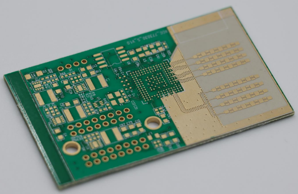
Open almost any electronic gadget — a phone, a TV remote, even a toy — and you’ll see a flat green board inside. That’s a printed circuit board, or PCB.
A PCB is like the heart and veins of an electronic device. It connects all the small parts — chips, resistors, and wires — so electricity can flow and the device can work.
Understanding how a PCB works helps you see how every modern device comes alive. Whether you’re fixing a gadget, building your own project, or just curious, learning about PCB boards, circuit board design, or printed wiring boards gives you a peek into the world inside your electronics.

What Is a Printed Circuit Board? (Definition & Core Function)
A printed circuit board (PCB) is a flat board that holds and connects all the electronic parts inside a device. Think of it like a small city for electricity — it gives a place for the parts to sit and safe roads for electricity to travel.
Mechanical Support for Components
PCBs provide a solid base for all electronic components. Without a PCB, tiny parts like chips, resistors, capacitors, and LEDs would float inside the device, making it fragile and easy to break. The board keeps each component in its correct spot and holds them tightly with solder, so the device stays reliable even when moved or dropped.
Electrical Connections with Copper Traces
Instead of using separate wires for every connection, PCBs use copper traces—thin lines of copper printed on the board—to carry electricity between components. These traces act like highways, guiding electric signals quickly and safely. Copper traces make the device smaller, lighter, and faster because everything is neatly connected on one board rather than a tangled mess of wires.
Common PCB Types
PCBs come in different types depending on how many layers of copper they have:
PCB Type | Description | Typical Use |
Single-sided | Copper traces on one side only | Simple electronics like calculators, toys, or small gadgets |
Double-sided | Copper traces on both sides | More complex circuits, like power supplies or LED boards |
Multilayer | Many layers of copper separated by insulating material | Advanced devices like smartphones, computers, and high-speed electronics |
Each type has a different structure that affects how electricity flows, how small the board can be, and how reliable it is. Learning PCB basics and how a PCB works helps you understand the hidden engineering inside every electronic device you use.

Inside the Layers: Anatomy of a PCB
A PCB isn’t just a flat green board. It is made of several layers stacked together, and each layer has a special job. Understanding these layers is like looking inside a cake—you can see the different parts that make the whole thing work.
Substrate / Core
The substrate, also called the core, is the main body of the PCB. Most boards use a material called FR-4, which is strong, lightweight, and does not conduct electricity. The substrate acts like the floor of a building, holding everything up. Some special PCBs use flexible materials or metal cores, allowing them to bend or handle higher power.
Copper Layers
On top of the substrate are the copper layers, which are the roads for electricity. These thin sheets of copper are etched to form paths, called traces, that carry electric signals between components. A single-layer board has copper on only one side, while a multilayer board has several copper layers stacked together, letting more complex circuits fit in a small space. The thickness of the copper affects how much current can safely flow.
Solder Mask
Covering the copper is the solder mask, usually green but sometimes blue, red, or black. This coating protects the copper from touching other parts or the environment. You can think of it like paint on a road, keeping traffic in the lanes.
Silkscreen
On top of the solder mask, the silkscreen adds white letters and symbols that identify components, pin numbers, and orientation. It works like street signs, helping engineers and makers place parts correctly.
Vias
Many PCBs have vias, tiny holes that connect layers together. Some go all the way through the board, while others connect only certain layers. Vias are like elevators, letting electricity travel between floors.
Layer Comparison Table
Layer | Function | Analogy |
Substrate / Core | Holds everything up | Floor of a building |
Copper | Conducts electricity | Roads or highways |
Solder Mask | Protects copper | Lane markings / paint |
Silkscreen | Shows labels and symbols | Street signs |
Vias | Connects layers | Elevators between floors |
By understanding these layers, you can see why some PCBs are simple, while others are powerful enough for smartphones, computers, or high-speed electronics. Every layer is carefully designed to make sure electricity flows safely and efficiently.

PCB Layout and Design Considerations
Before a PCB can be built, it needs a careful plan. The layout decides where each component goes and how electricity flows between them. A good layout makes the board reliable, efficient, and easier to manufacture.
From Schematic to Layout
Designing a PCB is like planning a small city for electricity. Every component and copper trace needs a clear path so the board works correctly. The process begins with a schematic, which is a map showing how all the components connect. The schematic ensures that power and signals flow correctly and that each part of the circuit works as intended. Once the schematic is complete, designers move to the layout stage. Here, they place each component on the board and carefully route the copper traces that connect them.
Trace Width and Spacing
The width of copper traces and the space between them are critical. Traces that are too thin can overheat or fail under heavy current, while traces placed too close together can cause short circuits. Proper planning of trace width and spacing ensures that electricity flows safely and reliably across the board.
Power and Ground Planes
Power and ground planes are large copper areas that provide stable voltage and a smooth return path for current. They reduce electrical noise and make the PCB more reliable. You can think of them like major highways in a city, carrying heavy traffic safely and efficiently.
Signal Integrity and EMI Considerations
High-speed signals on a PCB can interfere with each other if not carefully routed. Designers pay attention to signal integrity to make sure signals reach their destination without distortion. They also consider electromagnetic interference (EMI), using layout techniques to prevent unwanted noise that could affect the board or nearby devices.
Thermal Management
Some components generate heat during operation, so the layout must allow heat to dissipate properly. Designers may place heat-generating parts away from sensitive areas, use wider traces to carry current safely, or add thermal vias that transfer heat to other layers. Proper thermal management keeps the PCB stable and prevents failures.
EDA Tools for Layout
Designers use EDA (Electronic Design Automation) software to plan the layout, simulate the board, and check for errors before manufacturing. Popular tools include KiCad, Eagle, and Altium. Open-source tools like KiCad are especially popular among makers and hackers because they are free, flexible, and supported by a large community.
A carefully planned layout ensures that the PCB is reliable, easy to manufacture, and works as intended. Understanding PCB layout considerations allows makers to design their own boards, improve existing projects, and troubleshoot electronics effectively.

Manufacturing Process: From Design to Fabrication
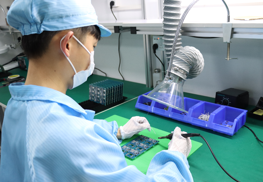
Before a PCB can power your gadget, it needs to be built carefully in a factory. The manufacturing process turns the design on a screen into a real board that can carry electricity and hold components reliably.
Design Verification and Preparation
Once the layout is complete, the first step is to check the design for errors. This includes verifying the schematic, testing trace widths, and making sure all connections are correct. Designers also prepare files called Gerbers, which tell the factory exactly how each layer of the PCB should be made.
Image Transfer and Etching
The copper layers are coated with a special film, and the circuit pattern is transferred onto them. Then, a chemical process called etching removes the unwanted copper, leaving only the traces that form the circuit. This step is like carving roads in a city map.
Drilling and Plating Vias
Holes are drilled where components will be placed or where different layers need to connect. Some holes go all the way through the board, while others connect only certain layers. After drilling, the holes are plated with copper so electricity can travel between layers.
Lamination
For multilayer PCBs, the different layers are stacked and fused together under heat and pressure. This lamination ensures the board is strong, flat, and electrically stable.
Solder Mask and Silkscreen
Next, the board is coated with a solder mask to protect the copper traces. Then the silkscreen is printed on top, showing component labels, pin numbers, and helpful symbols. These steps make the board easier to assemble and reduce mistakes.
Surface Finish
A surface finish is applied to the copper pads so solder sticks properly when components are added. Common finishes include HASL (Hot Air Solder Leveling), ENIG (Electroless Nickel Immersion Gold), and OSP (Organic Solderability Preservative).
Testing and Inspection
Finally, the PCB is tested to make sure all connections are correct and there are no short circuits. Electrical testing and visual inspections catch mistakes before the board is shipped.
Every step in manufacturing is carefully controlled to ensure that the final PCB works as intended. Understanding the PCB fabrication process helps makers and engineers appreciate the hidden craftsmanship inside every electronic device.

Advanced PCB Technologies (Optional Bonus Section)
As electronics become faster and more complex, simple PCBs are no longer enough. Advanced PCB technologies are designed to handle high-speed signals, complex circuits, and challenging environments. These boards are used in devices like 5G equipment, electric vehicles (EVs), aerospace systems, and other high-performance electronics.
High-Speed and HDI PCBs
High-speed PCBs are designed to carry signals that change very quickly. At these speeds, even small imperfections in the traces can cause signal loss or interference. HDI (High-Density Interconnect) PCBs use very small traces and vias to fit more connections in a smaller area. Think of them as tiny expressways for electricity, allowing complex circuits to operate reliably in a compact space.
Rigid-Flex and Metal Core PCBs
Some devices need PCBs that can bend or handle heat better. Rigid-flex PCBs combine rigid boards with flexible sections, making them perfect for wearable devices, foldable gadgets, and space-constrained electronics. Metal core PCBs use a metal base to dissipate heat quickly, ideal for LED lighting, power electronics, or devices that generate a lot of heat.
Special Materials for High-Frequency Applications
Advanced PCBs often use special materials like Rogers, Megtron, or Isola. These materials maintain signal integrity at high frequencies, making them essential for RF (radio frequency) boards, high-speed networking, and 5G applications. They reduce signal loss and prevent interference that standard FR-4 boards cannot handle.
These advanced PCB technologies allow modern electronics to be smaller, faster, and more reliable. By understanding advanced PCBs, high-speed PCBs, and rigid-flex PCBs, makers and engineers can appreciate the engineering that goes into the devices we rely on every day.

Why PCBs Matter for Hackers and Makers
Before you start building or tinkering, it’s important to understand why PCBs are so essential. They are not just parts you buy—they are the foundation that makes your projects work reliably and efficiently.
PCBs Are the Heart of Every Project
PCBs are the backbone of every electronic device. For hackers, makers, and DIY enthusiasts, understanding how PCBs work opens the door to designing, building, and improving their own projects. A well-designed PCB organizes components neatly, reduces errors, and makes circuits more reliable. Even simple hobby projects, like a custom LED controller or a small robot, benefit from using a proper PCB.
Learning Through Open-Source Communities
Many makers turn to open-source hardware communities for guidance and inspiration. Platforms like OSH Park, PCBWay shared projects, and KiCad forums offer free designs, tutorials, and tools. By exploring these resources, beginners and experts alike can learn how to take a concept from paper to a fully functional PCB.
Exploring Advanced Technologies
PCBs also allow makers to experiment with more advanced technologies. By trying high-speed boards, rigid-flex PCBs, or multilayer designs, hobbyists can explore professional-level electronics in a DIY setting. Understanding PCBs gives makers the ability to solve problems creatively, improve device performance, and innovate—skills that are at the core of Hackaday’s maker culture.

Conclusion: The Hidden Art Inside Every Device
Every electronic device you use hides a carefully designed PCB inside. These boards are what connect and organize all the tiny components, making the device work reliably. From the layers and layout to advanced manufacturing processes, each PCB is a combination of engineering skill and thoughtful design.
Understanding how PCBs work gives you a new appreciation for the electronics around you. It also opens opportunities for makers, hackers, and engineers to create, experiment, and innovate. The next time you open a gadget, you’ll see more than a green board—you’ll see the hidden art that brings technology to life.
 pcbmaster
Discussions
Become a Hackaday.io Member
Create an account to leave a comment. Already have an account? Log In.