-
What Printed Circuit Board Images Can Tell You: Hidden Signals Behind Every Trace
4 days ago • 0 comments![]()
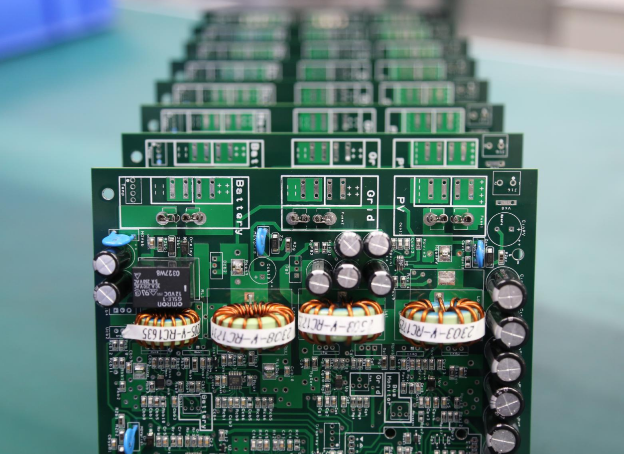
If you spend enough time ripping apart old hardware, you eventually realize something: printed circuit board images contain far more engineering truth than the datasheet ever admits. For hardware hackers, reverse-engineers, and anyone who enjoys the sight of neatly routed copper, PCB photography has quietly become one of the most useful analysis tools.
High-resolution board photos — optical, X-ray, or even macro shots from a smartphone — reveal layout decisions, high-speed design rules, EMI mitigation tricks, and manufacturing shortcuts. In many cases, a single well-lit image exposes more about a circuit’s performance limits than a multi-page “theoretical” design guide.
In this article, we’ll walk through what engineers and hackers can extract from printed circuit board images, how to read them like a seasoned designer, and why photography has evolved into an essential part of modern reverse engineering.
Reading a PCB Image Like a Hardware Hacker
Most people see a PCB photo as… well, a pretty picture of copper and fiberglass. But an experienced engineer sees a map of decisions made by someone optimizing cost, manufacturability, signal integrity, and sometimes pure desperation.
From a single top-layer photo, you can infer:
- Power distribution routes
- Grounding and return path strategy
- Component placement logic
- Controlled-impedance routing
- RF shielding boundaries
- Layer-stack decisions (yes, you can guess from the surface)
Add a bottom-layer photo, and the story becomes even clearer. And once you bring in X-ray images for BGA or microvia structures, nearly the entire stack-up becomes visible.
Reverse Engineering: Rebuilding Logic from Images
Using printed circuit board images for reverse engineering is no longer a niche hacker skill — it’s standard practice in hardware security analysis.
With good photography, you can:
- Reconstruct net connections
- Identify differential pairs
- Detect hidden bodge wires and late-stage fixes
- Determine the impedance strategy
- Map out power rails and voltage domains
- Spot “security through obscurity” patterns (decoy vias, shielded traces, etc.)
Tools like KiCad, OpenCV, and even AI-based trace extractors can convert 2D images into vectorized PCB layers. Combine multiple high-resolution shots with a bit of detective work, and you can rebuild a nearly complete schematic.
High-Speed PCB Design Details Hidden in Plain Sight
Sometimes you don’t need a TDR or VNA to understand a high-speed signal path — a zoomed-in PCB image tells the whole story.
Here’s what high-speed PCB design principles look like when “visually decoded”:
1. Differential pair matching
Uneven trace lengths show up immediately. Even a 0.5 mm mismatch is visible as serpentine wiggles. If the wiggles are missing, you know the designer didn’t care about high-speed timing — or didn’t know better.
2. Impedance control
You can identify controlled-impedance traces by their consistent width and uniform spacing from nearby copper. On a poorly designed board, widths vary and return paths get chopped up.
3. Over-via’d signals
A differential pair jumping through seven vias in 5 cm? That’s a performance problem waiting to happen. High-speed engineers usually minimize via count — photos reveal immediately who respected that rule.
4. Reference plane quality
Cutouts, splits, and ground-plane islands show up clearly in images. These often correlate directly with EMI hotspots.
A high-speed PCB doesn’t just function — it looks high-speed.
EMI Shielding and Grounding Clues Hidden in the Copper
Printed circuit board images reveal EMI failures long before anyone brings out a spectrum analyzer. From a single picture, you can spot:
- Shield cans with incomplete grounding
- Long unbroken loops (accidental antennas)
- Missing stitching vias
- Gaps between analog and digital return paths
- Over-isolated sections causing return-path disasters
Single-side...
Read more » -
How to Choose Free PCB Design Software for Advanced Printed Circuit Boards
11/13/2025 at 08:21 • 0 commentsEvery electronic device starts with a printed circuit board, or PCB. It’s the heart that connects every component and makes the system work. To design one, engineers use special tools called PCB design software.
Today, there are many free PCB design software for advanced printed circuit boards, and that’s great news for makers and small teams. But choosing the right one is not easy. Some tools are perfect for simple LED blinkers; others can handle high-speed signals and 16-layer boards.
The trick is to balance cost, capability, and complexity. A good free tool can take your design from idea to working prototype — if you pick wisely.

What “Free” Really Means in PCB Design Software
When you see the word “free,” it sounds great — but in PCB design, “free” can mean a few very different things. Let’s break it down in simple terms.
First, there are truly free tools. These are often open-source PCB CAD programs, like KiCad. You can download them, use them for any kind of project, even sell boards you design — and you never pay a cent. The trade-off? They might take more time to learn, and you’ll rely on the user community for help instead of company support.
Next, there are freemium EDA tools. “Freemium” means you get a basic version for free, but advanced features cost money. For example, a free plan might limit how many layers your board can have or how big it can be. You can design small hobby projects, but not a high-speed multilayer board. It’s a taste of the full product, not the whole meal.
Finally, some tools are free only for personal or non-commercial use. That means you can’t use them for paid or company projects without buying a license.
So yes, free tools aren’t magic — but some are surprisingly capable. If you understand what “free” really means and match the tool to your project, you can still create powerful designs without spending a dollar.

Key Factors to Evaluate When Choosing Free PCB Design Software
When you pick a free PCB design tool, don’t just look at the price — look at what it can really do. Here are the most important things to check before you start your next board.
1. Design Complexity Support
If your project has many layers or high-speed signals, you need software that can handle multilayer boards, HDI layouts, and differential pairs. Some free tools only support 2 layers, which is fine for simple circuits. But if you want to design advanced printed circuit boards — like those used in routers or computers — you’ll need tools that allow impedance control and more complex routing options.
2. Library and Footprint Management
Every part on your board needs a symbol and a footprint. Good software helps you find, edit, or build these easily. Some tools have cloud libraries with thousands of ready-to-use parts, which saves a lot of time. Others let you make your own custom libraries, which is useful for rare or new components. Just make sure your software can import and export these files easily.
3. Simulation and Verification Tools
Before sending your design to a factory, you must be sure it works. Free PCB design software should include tools like DRC (Design Rule Check), signal integrity checks, and sometimes thermal analysis. These tools catch mistakes early — like tracks that are too close or missing connections — and can save you time and money later.
4. Manufacturing File Output
Once your design is ready, you need to send it to a PCB manufacturer. Your software must export Gerber files, drill files, and ideally ODB++ or IPC-2581 formats. Also, check if it supports stack-up management, which defines the thickness and material of each layer. If your tool can’t output standard manufacturing files, your project may stop before it even starts.
5. Community and Documentation
With open-source PCB CAD tools, community support is everything. You’ll find help in forums, YouTube tutorials, and online guides....
Read more » -
What Is a Printed Circuit Board? Inside the Layers, Layouts & Manufacturing Process
11/06/2025 at 08:18 • 0 commentsOpen almost any electronic gadget — a phone, a TV remote, even a toy — and you’ll see a flat green board inside. That’s a printed circuit board, or PCB.
A PCB is like the heart and veins of an electronic device. It connects all the small parts — chips, resistors, and wires — so electricity can flow and the device can work.
Understanding how a PCB works helps you see how every modern device comes alive. Whether you’re fixing a gadget, building your own project, or just curious, learning about PCB boards, circuit board design, or printed wiring boards gives you a peek into the world inside your electronics.
 showing layers, layout, and manufacturing process for electronics.")
What Is a Printed Circuit Board? (Definition & Core Function)
A printed circuit board (PCB) is a flat board that holds and connects all the electronic parts inside a device. Think of it like a small city for electricity — it gives a place for the parts to sit and safe roads for electricity to travel.
Mechanical Support for Components
PCBs provide a solid base for all electronic components. Without a PCB, tiny parts like chips, resistors, capacitors, and LEDs would float inside the device, making it fragile and easy to break. The board keeps each component in its correct spot and holds them tightly with solder, so the device stays reliable even when moved or dropped.
Electrical Connections with Copper Traces
Instead of using separate wires for every connection, PCBs use copper traces—thin lines of copper printed on the board—to carry electricity between components. These traces act like highways, guiding electric signals quickly and safely. Copper traces make the device smaller, lighter, and faster because everything is neatly connected on one board rather than a tangled mess of wires.
Common PCB Types
PCBs come in different types depending on how many layers of copper they have:
PCB Type
Description
Typical Use
Single-sided
Copper traces on one side only
Simple electronics like calculators, toys, or small gadgets
Double-sided
Copper traces on both sides
More complex circuits, like power supplies or LED boards
Multilayer
Many layers of copper separated by insulating material
Advanced devices like smartphones, computers, and high-speed electronics
Each type has a different structure that affects how electricity flows, how small the board can be, and how reliable it is. Learning PCB basics and how a PCB works helps you understand the hidden engineering inside every electronic device you use.
 with components illustrating PCB structure, definition, and core function.")
Inside the Layers: Anatomy of a PCB
A PCB isn’t just a flat green board. It is made of several layers stacked together, and each layer has a special job. Understanding these layers is like looking inside a cake—you can see the different parts that make the whole thing work.
Substrate / Core
The substrate, also called the core, is the main body of the PCB. Most boards use a material called FR-4, which is strong, lightweight, and does not conduct electricity. The substrate acts like the floor of a building, holding everything up. Some special PCBs use flexible materials or metal cores, allowing them to bend or handle higher power.
Copper Layers
On top of the substrate are the copper layers, which are the roads for electricity. These thin sheets of copper are etched to form paths, called traces, that carry electric signals between components. A single-layer board has copper on only one side, while a multilayer board has several copper layers stacked together, letting more complex circuits fit in a small space. The thickness of the copper affects how much current can safely flow.
Solder Mask
Covering the copper is the solder mask, usually green but sometimes blue, red, or black. This coating protects the copper from touching other parts or the environment. You can think of it like paint on a road, keeping traffic in the lanes.
Silkscreen
On top of the solder mask, the silkscreen adds white letters and symbols that identify components, pin numbers, and orientation. It works like...
Read more »


 showing layers, layout, and manufacturing process for electronics.")
 with components illustrating PCB structure, definition, and core function.")
 Eric Tsai
 U.S. Water Rockets
 Lutetium
 Luke Beno
 Rui Santos
 Michiel Spithoven
 Afrdt
Afrdt NASCO
NASCO pRoFiT
 Jaime García
 Colby Johnson
 Boian Mitov
 Marius Taciuc
 Cedric Honnet