 pcbmaster
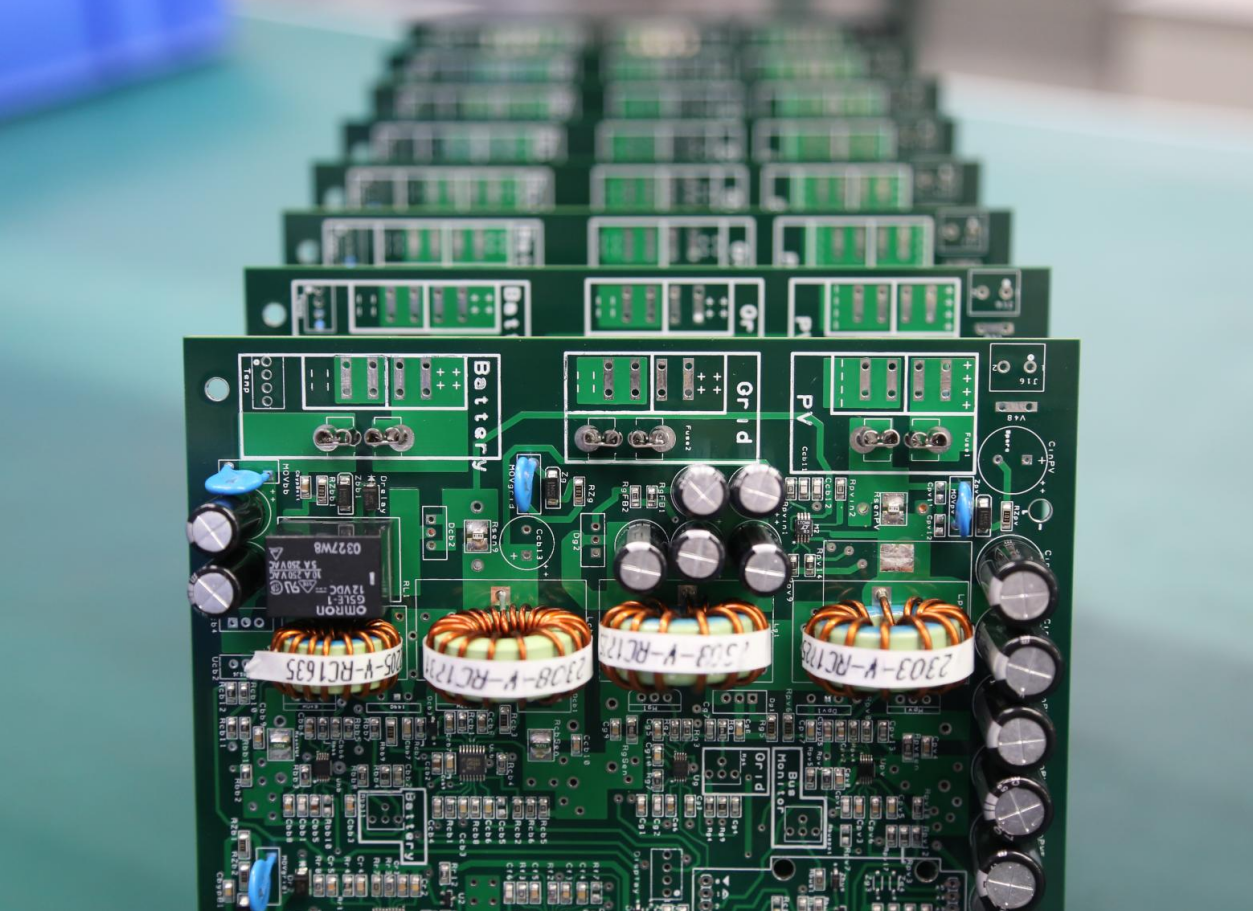
If you spend enough time ripping apart old hardware, you eventually realize something: printed circuit board images contain far more engineering truth than the datasheet ever admits. For hardware hackers, reverse-engineers, and anyone who enjoys the sight of neatly routed copper, PCB photography has quietly become one of the most useful analysis tools.
High-resolution board photos — optical, X-ray, or even macro shots from a smartphone — reveal layout decisions, high-speed design rules, EMI mitigation tricks, and manufacturing shortcuts. In many cases, a single well-lit image exposes more about a circuit’s performance limits than a multi-page “theoretical” design guide.
In this article, we’ll walk through what engineers and hackers can extract from printed circuit board images, how to read them like a seasoned designer, and why photography has evolved into an essential part of modern reverse engineering.
Reading a PCB Image Like a Hardware Hacker
Most people see a PCB photo as… well, a pretty picture of copper and fiberglass. But an experienced engineer sees a map of decisions made by someone optimizing cost, manufacturability, signal integrity, and sometimes pure desperation.
From a single top-layer photo, you can infer:
- Power distribution routes
- Grounding and return path strategy
- Component placement logic
- Controlled-impedance routing
- RF shielding boundaries
- Layer-stack decisions (yes, you can guess from the surface)
Add a bottom-layer photo, and the story becomes even clearer. And once you bring in X-ray images for BGA or microvia structures, nearly the entire stack-up becomes visible.
Reverse Engineering: Rebuilding Logic from Images
Using printed circuit board images for reverse engineering is no longer a niche hacker skill — it’s standard practice in hardware security analysis.
With good photography, you can:
- Reconstruct net connections
- Identify differential pairs
- Detect hidden bodge wires and late-stage fixes
- Determine the impedance strategy
- Map out power rails and voltage domains
- Spot “security through obscurity” patterns (decoy vias, shielded traces, etc.)
Tools like KiCad, OpenCV, and even AI-based trace extractors can convert 2D images into vectorized PCB layers. Combine multiple high-resolution shots with a bit of detective work, and you can rebuild a nearly complete schematic.
High-Speed PCB Design Details Hidden in Plain Sight
Sometimes you don’t need a TDR or VNA to understand a high-speed signal path — a zoomed-in PCB image tells the whole story.
Here’s what high-speed PCB design principles look like when “visually decoded”:
1. Differential pair matching
Uneven trace lengths show up immediately. Even a 0.5 mm mismatch is visible as serpentine wiggles. If the wiggles are missing, you know the designer didn’t care about high-speed timing — or didn’t know better.
2. Impedance control
You can identify controlled-impedance traces by their consistent width and uniform spacing from nearby copper. On a poorly designed board, widths vary and return paths get chopped up.
3. Over-via’d signals
A differential pair jumping through seven vias in 5 cm? That’s a performance problem waiting to happen. High-speed engineers usually minimize via count — photos reveal immediately who respected that rule.
4. Reference plane quality
Cutouts, splits, and ground-plane islands show up clearly in images. These often correlate directly with EMI hotspots.
A high-speed PCB doesn’t just function — it looks high-speed.
EMI Shielding and Grounding Clues Hidden in the Copper
Printed circuit board images reveal EMI failures long before anyone brings out a spectrum analyzer. From a single picture, you can spot:
- Shield cans with incomplete grounding
- Long unbroken loops (accidental antennas)
- Missing stitching vias
- Gaps between analog and digital return paths
- Over-isolated sections causing return-path disasters
Single-side EMI shields appear as simple copper regions. Double-sided shields look more like a continuous Faraday cage tied down by dense via grids. Flex PCB shielding is often a laminated foil; cracks or delamination are actually visible in photographs.
If a board fails EMC testing, you can often point to the image and say, “Yep. That’s why.”
Signal Integrity Mistakes You Can See Without Any Instrumentation
Printed circuit board images tell the story of signal integrity triumphs — and disasters.
Common issues visible in photos:
- Stub traces left behind by unused vias
- Tightly clustered vias causing impedance spikes
- 90-degree trace corners (purely aesthetic and purely harmful at high speed)
- Crosstalk risk: long parallel traces with insufficient spacing
- Poor termination placement, often centimeters away from the driver
You don’t need an oscilloscope to know the waveform is ugly — the board’s artwork already gave it away.
What Flexible Circuit Images Reveal About Reliability
Flex PCBs make things interesting because the mechanical and electrical domains overlap. Their printed circuit board images can show:
- Cracked copper due to too-tight bend radius
- Broken shield films
- Delamination or adhesive bubbles
- Poorly reinforced stiffener regions
- Misaligned coverlay
Flex circuits age fast when stressed improperly. A single magnified photo often predicts long-term failure.
Manufacturing Insights Visible in Any Multilayer PCB Image
You can tell more about a manufacturer’s quality from images than from their marketing brochure.
For example:
- Microvia alignment shows whether the drill process is tightly controlled
- Copper thickness becomes obvious at cut edges
- Solder mask registration reveals the factory’s process accuracy
- Uneven ENIG plating shows inconsistencies in chemical baths
- BGA pad quality under X-ray reveals voiding, cold joints, or misalignment
Even the presence of subtle burn marks or brownish resin tones gives clues about lamination pressure and heat history.
DIY Tools for Capturing High-Quality PCB Images
You do NOT need a $2,000 microscope to capture useful PCB imagery. Hackers have built high-quality imaging rigs using:
- A smartphone + a $10 macro lens
- A 3D-printed focusing frame
- A ring of LED strip lights
- A repurposed document scanner for flat PCB shots
- A $20 USB microscope for via inspection
Good lighting and stable mounting matter more than expensive optics.
With a bit of image stacking, you can get near-microscope clarity from consumer hardware.
Community Favorites: The Most Interesting PCB Images Found in the Wild
Hardware enthusiasts have shared some legendary PCB images over the years:
- Art-level trace patterns from vintage Japanese audio gear
- Sensor boards designed like city roadmaps
- Horrific low-cost router PCBs with single-point ground nightmares
- Flex circuits folded in origami-like shapes inside smartphones
- RF sections that look like miniature mazes
PCB images are not just diagnostic tools — they’re a form of engineering art. And they tell stories, sometimes better than documentation.
Conclusion: Every PCB Image Is a Blueprint Waiting to Be Decoded
Printed circuit board images are more than photography. They are:
- Reverse-engineering maps
- High-speed signal integrity diagrams
- EMI predictors
- Manufacturing fingerprints
- Reliability clues
- Aesthetic engineering artifacts
- And sometimes, hacker treasure maps
If you know how to read them, a single picture can reveal everything that matters about a design — its strengths, its weaknesses, and its philosophy.
In the world of hardware hacking, PCB images are not just pictures.
They’re the truth.
Discussions
Become a Hackaday.io Member
Create an account to leave a comment. Already have an account? Log In.