 ElecLab
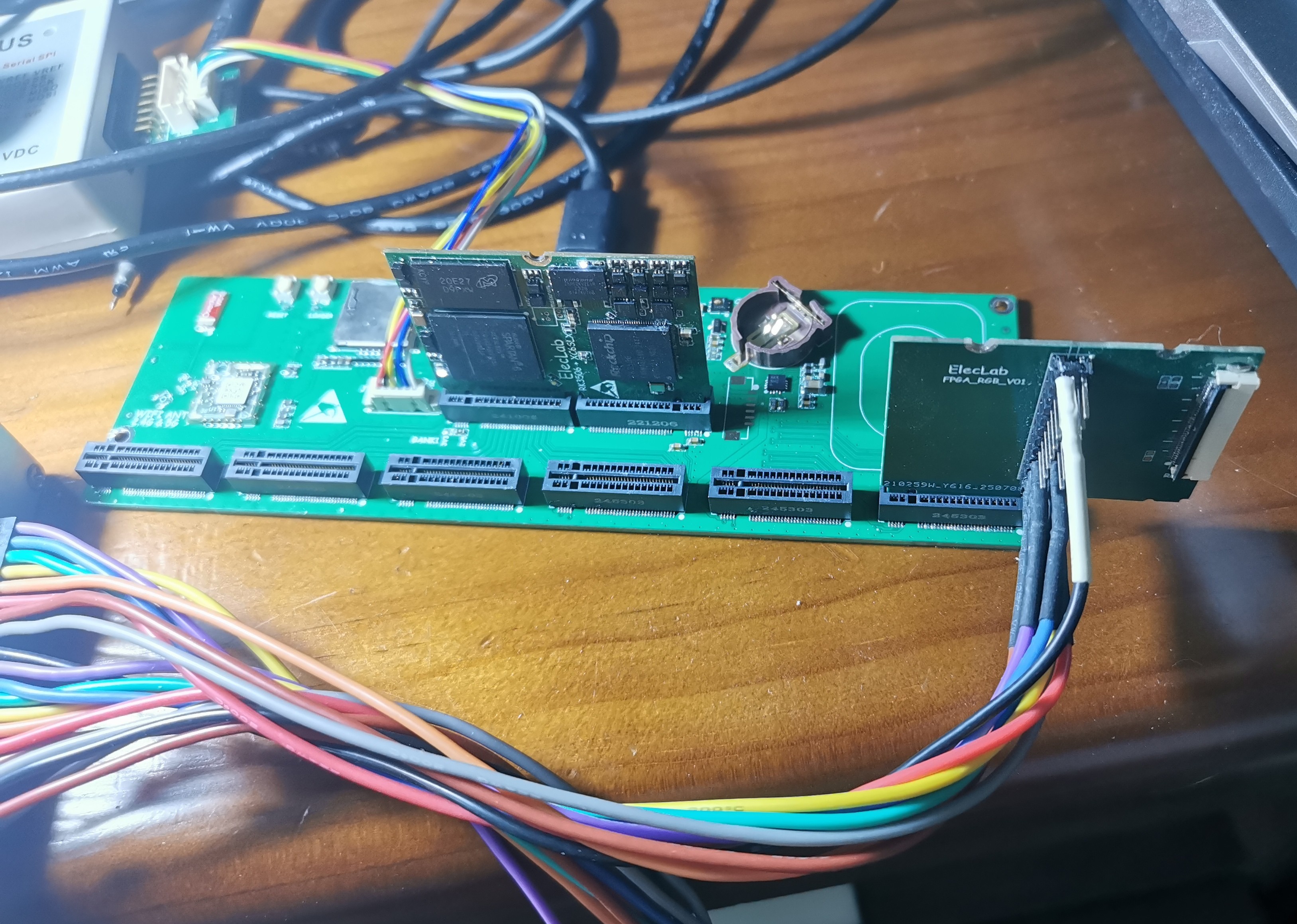
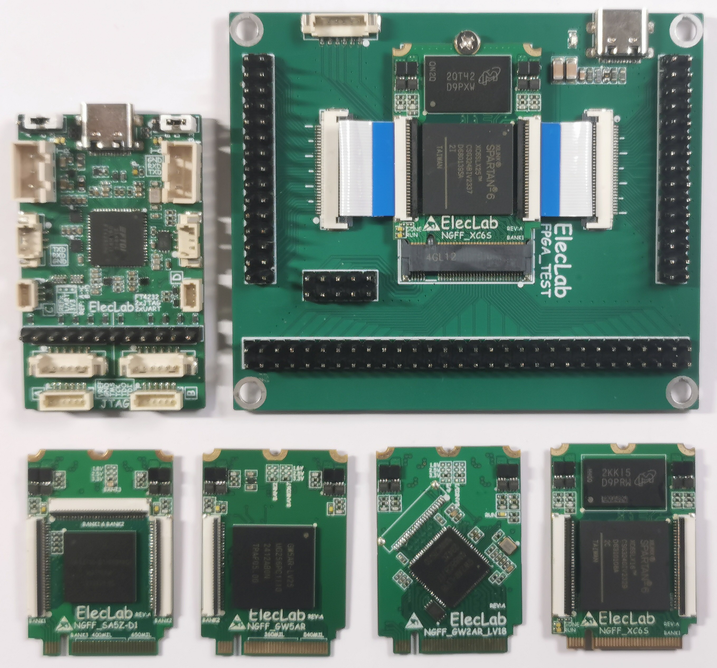
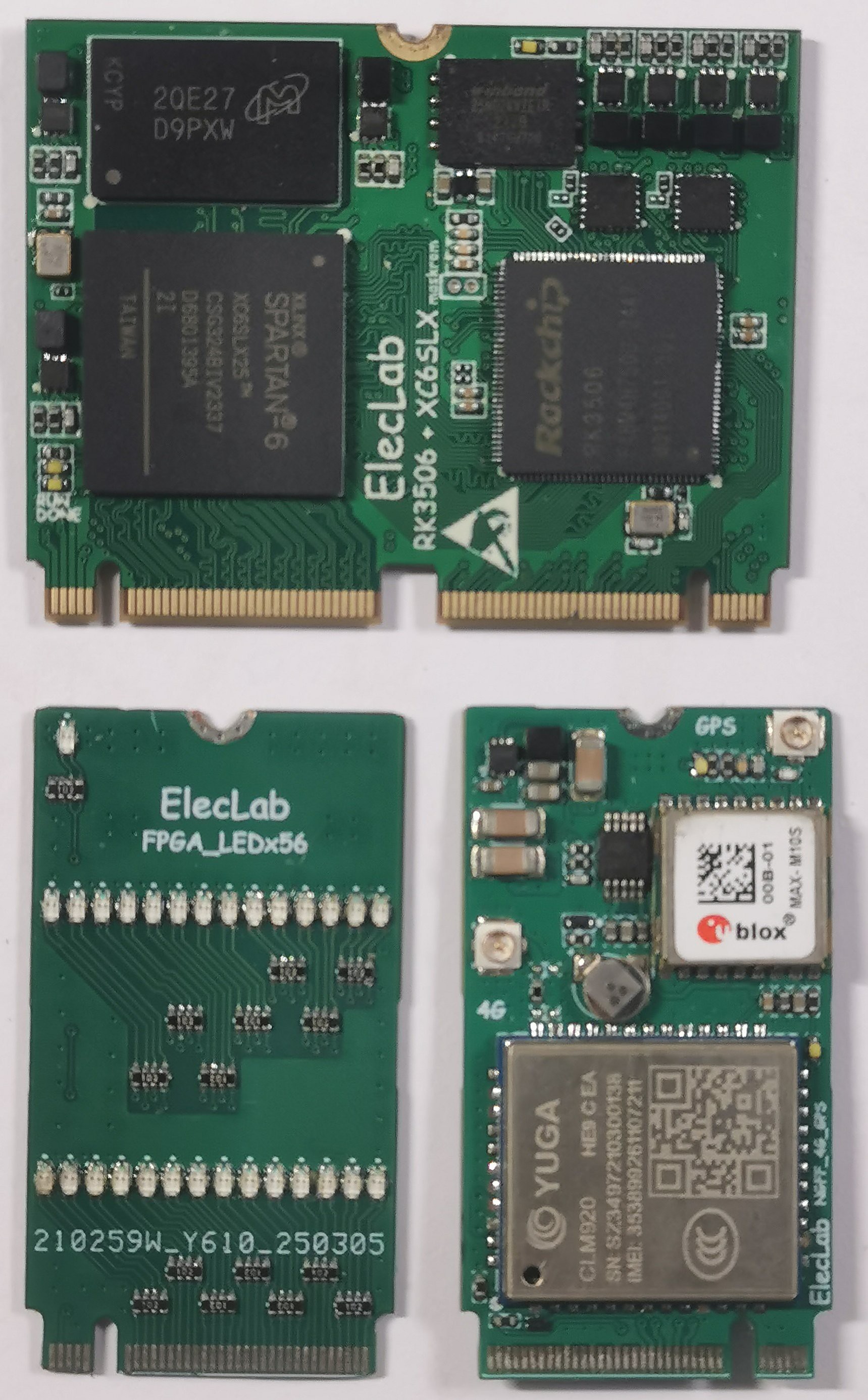
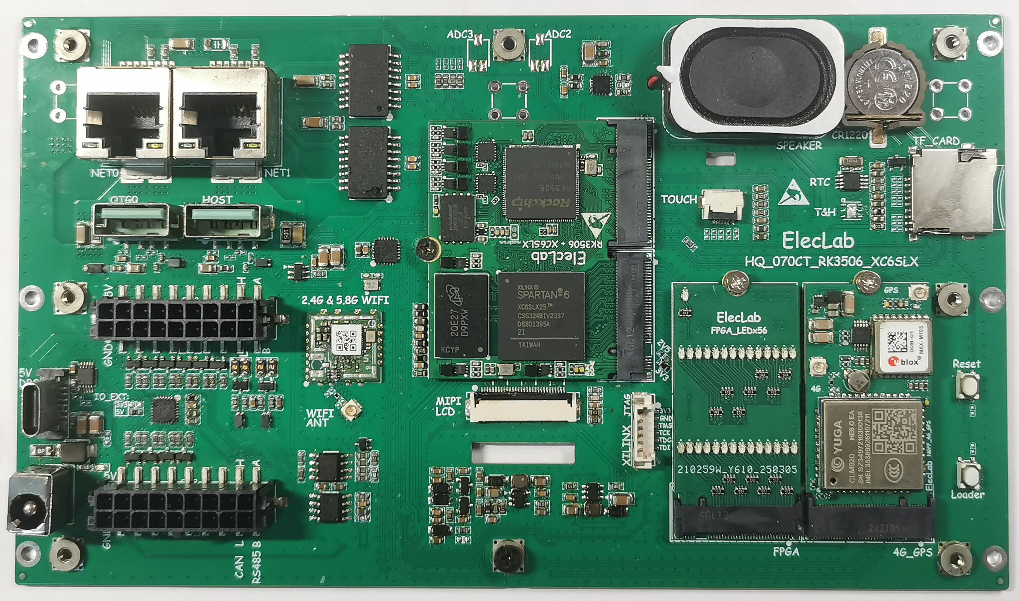
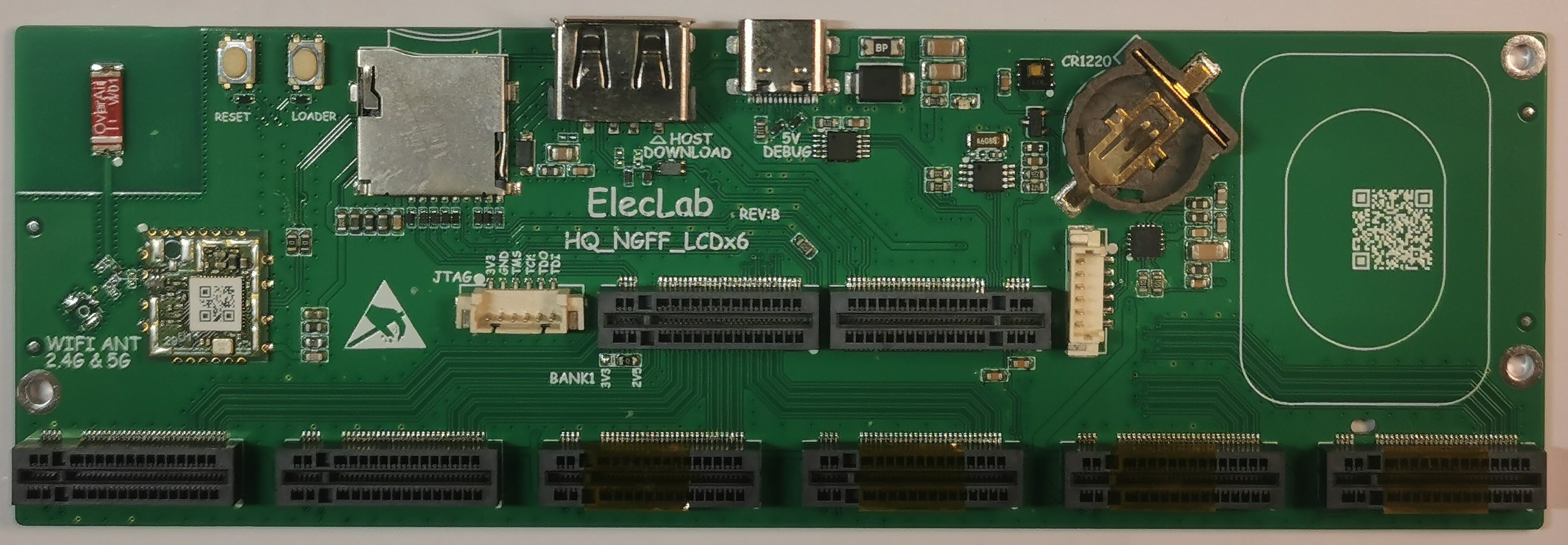
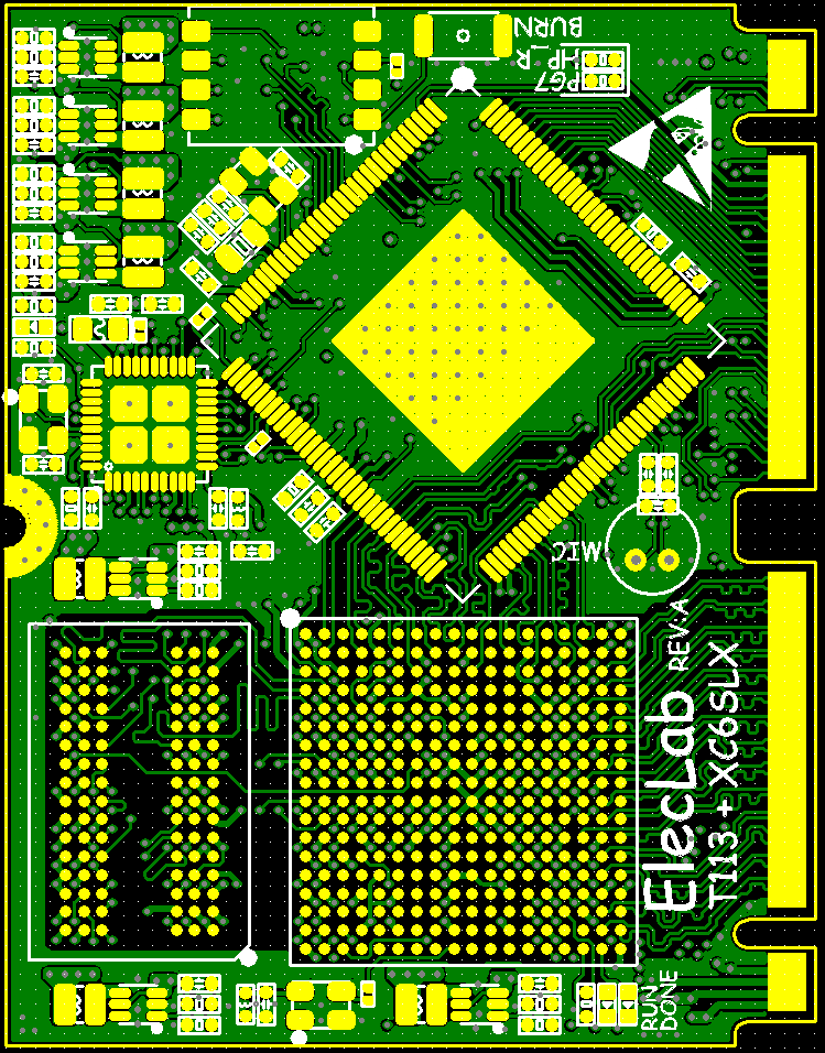
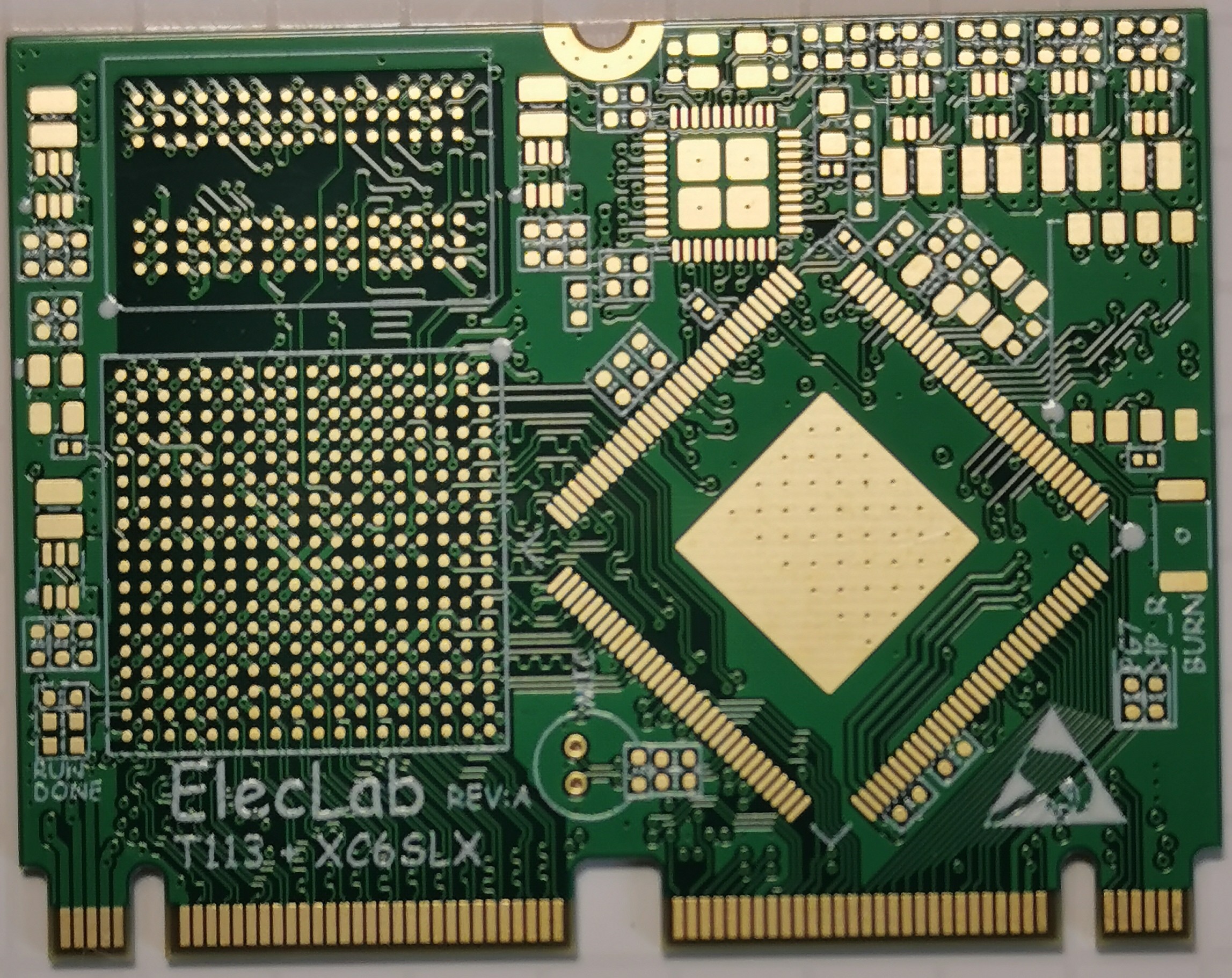
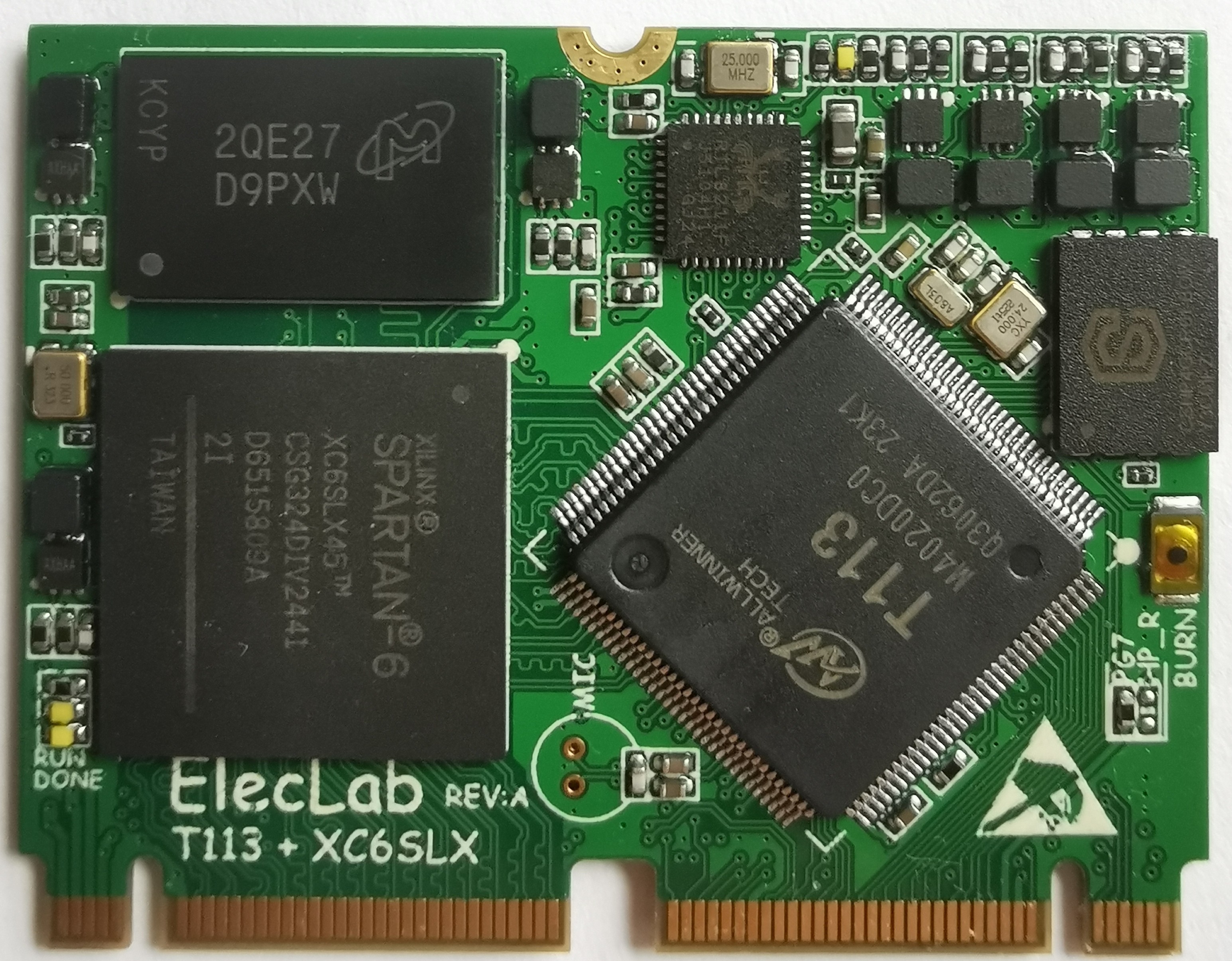
1. RockChip's newly released RK3506G2 QFN128 chip, which includes 3x1.5GHz Cortex-A7+ 200MHz Cortex-M0 and 2x 100MMAC and built-in 128M DDR3L. It has a set of 16bits 150MHz DDR data transmission DSMC bus interface (which multiplexes with 24bits RGB interface) and 2Lanes MIPI DSI interface. It can run Linux 6.1 or Preempt-RT real-time system + RTOS. We use its DSMC/RGB interface to connect xilinx's XC6SLX25 FPGA chip, making it more suitable for various applications for various flexible interfaces. For example, the application of metering/ADC/DAC/DDS/video. The second is to use Allwinner's T113-S4+XC6SLX25, which has built-in 256M DDR3 and Gigabit MAC and 1080P decoding capabilities. We use 2xLVDS to connect to XC6SLX25, enabling it to output 1920x1080 video signals.
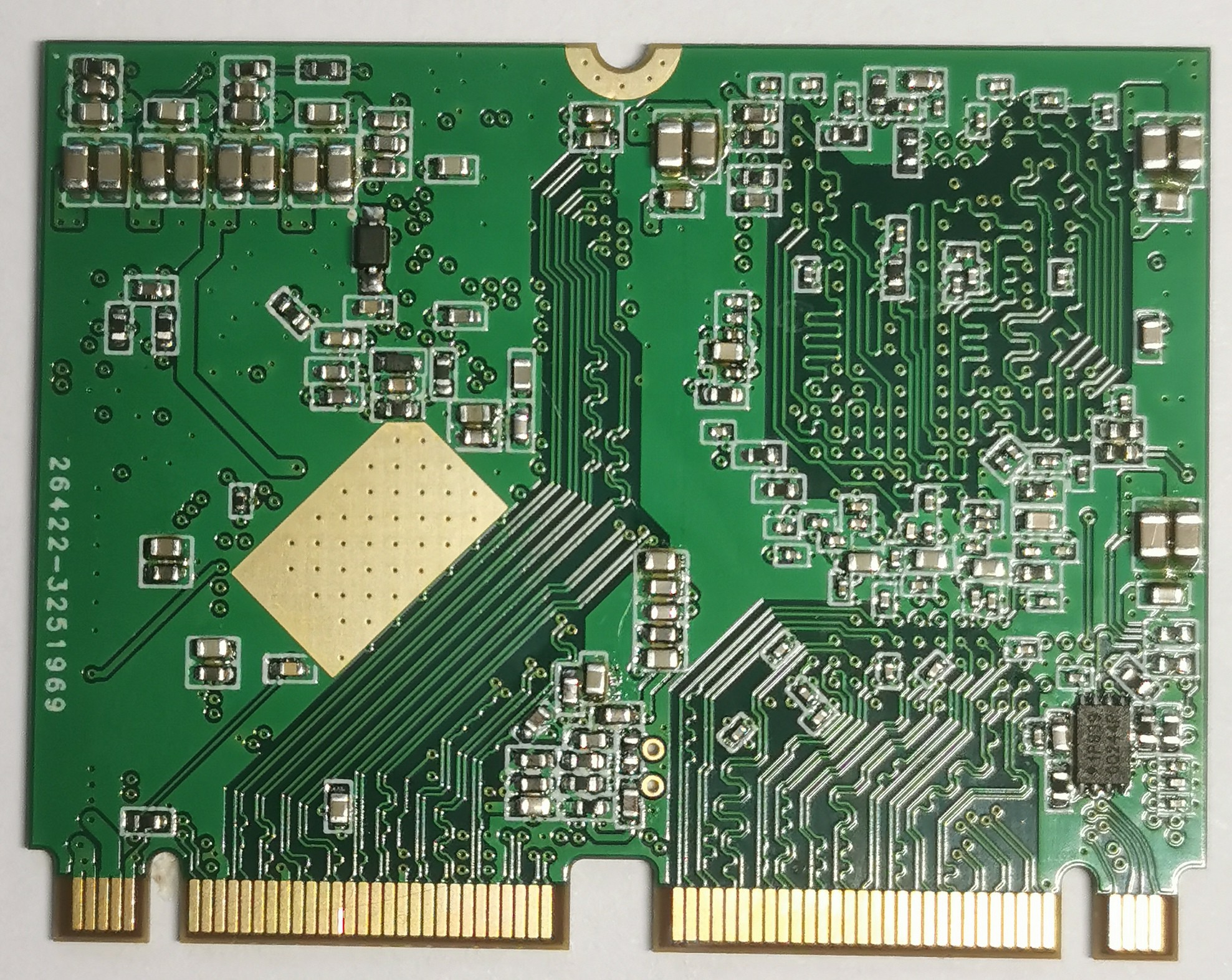
2. We have also designed several very interesting FPGA small boards with NGFF interfaces, which can be replaced directly. They are XC6SLX16/25/45+667Mbps 512MBytes DDR3 and 28nm XC7S50+800Mbps 512MBytes DDR3L and GW2AR-LV18 QFN88 package integration 20K LUT and 166MHz 64Mbit 32bits SDRAM and 22nm GW5AR-LV25 BGA256 package integration 23K LUT and 1066Mbps 128Mbits 16bits HyperRAM and 28nm SA5Z-30-D1 BGA213 package integration 32K LUT and 800Mbps 128Mbits DDR2+200M Cortex-M3. Next, several models will be designed, such as the 16 nm model and the LPDDR3/LPDDR4 interface.
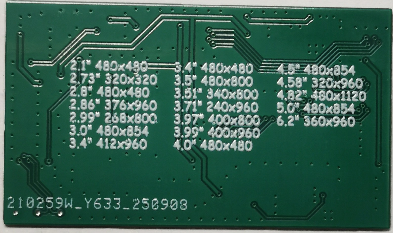
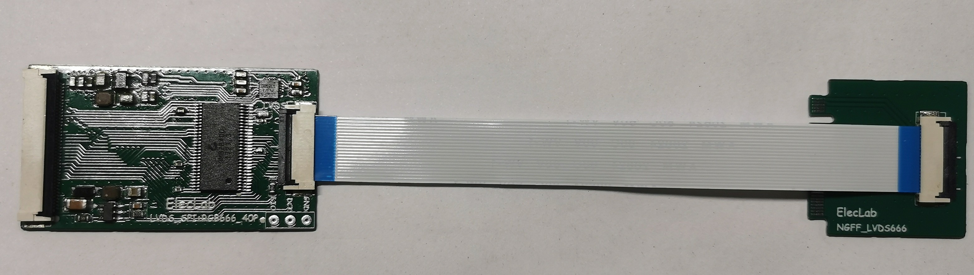
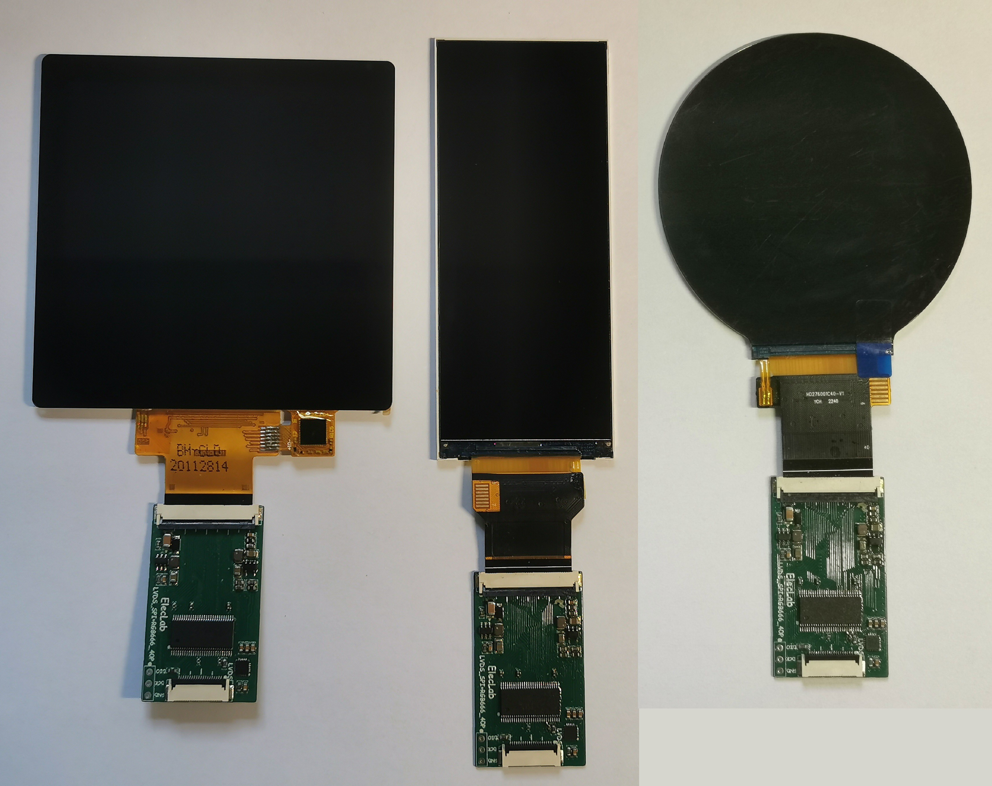
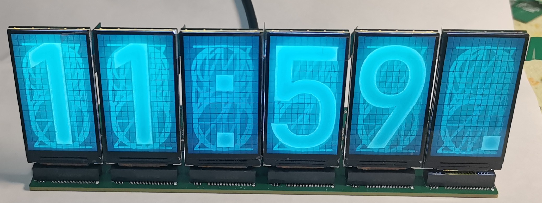
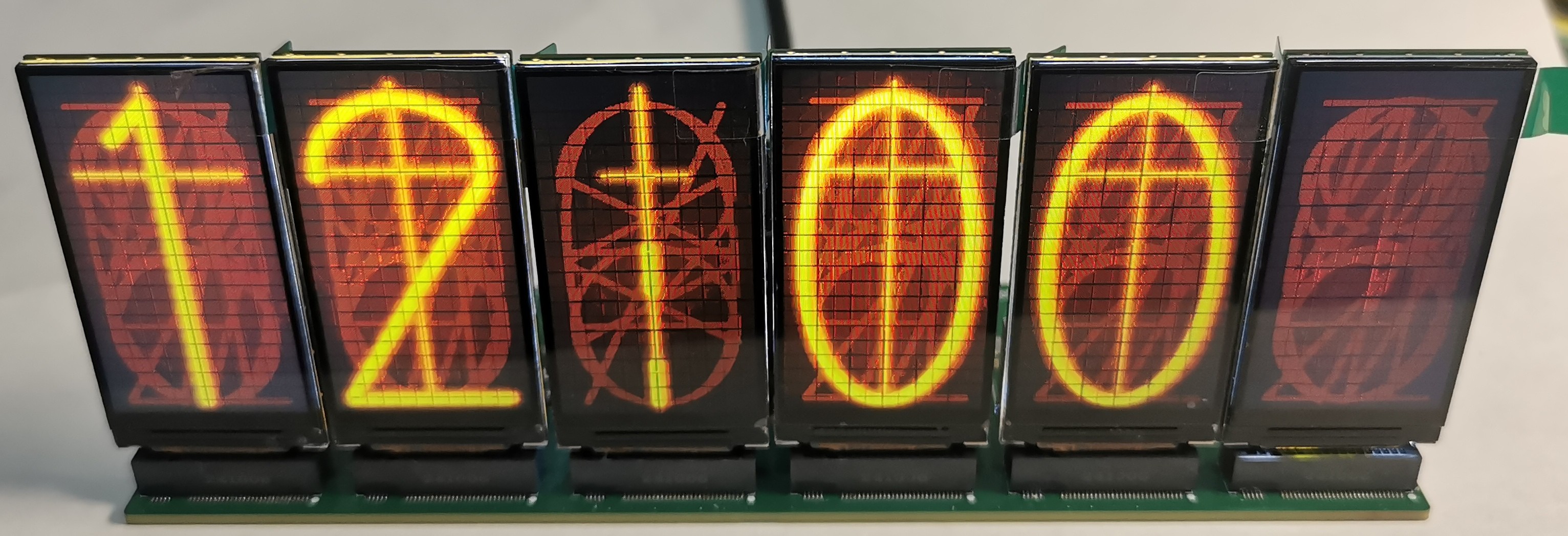
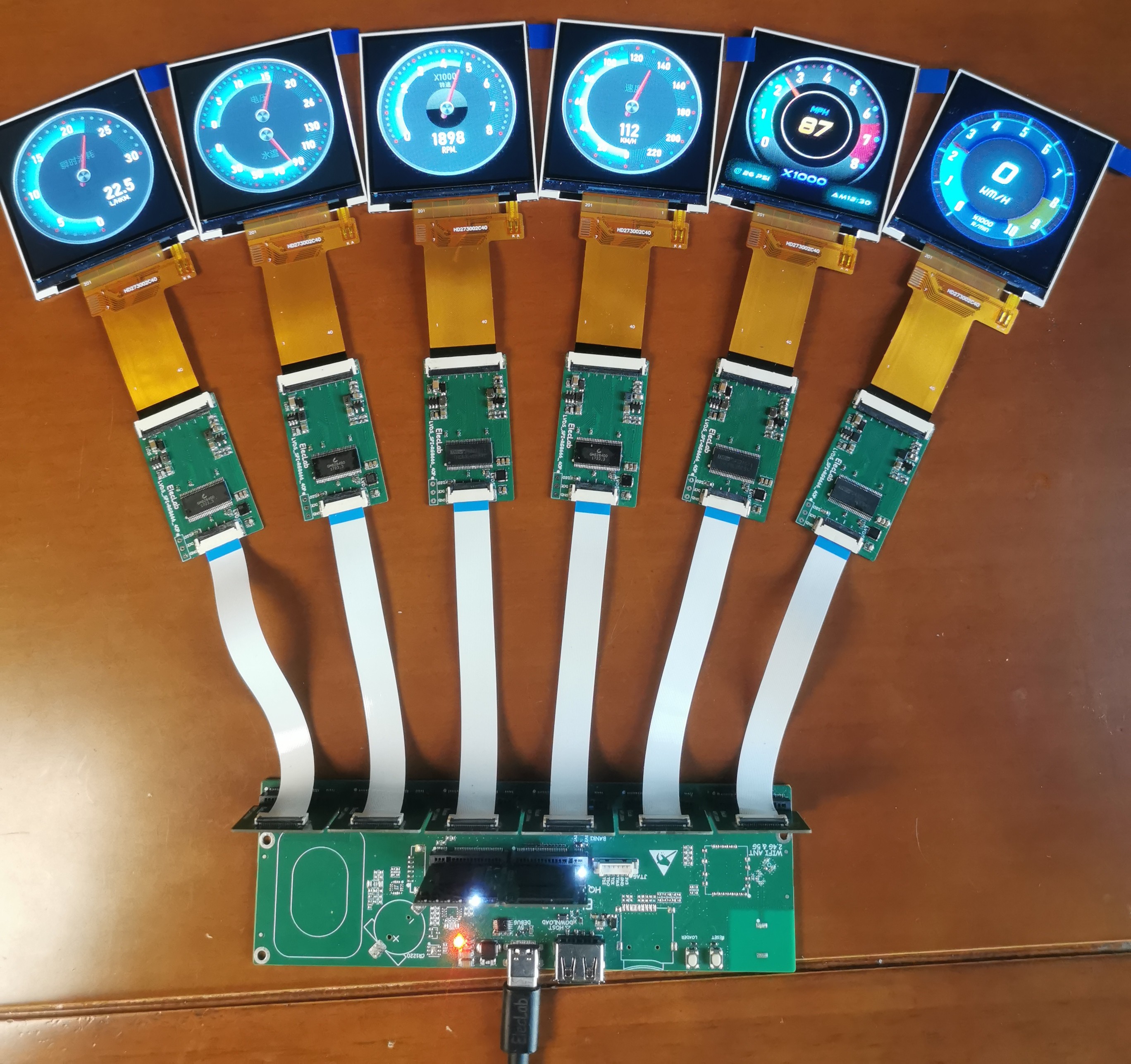
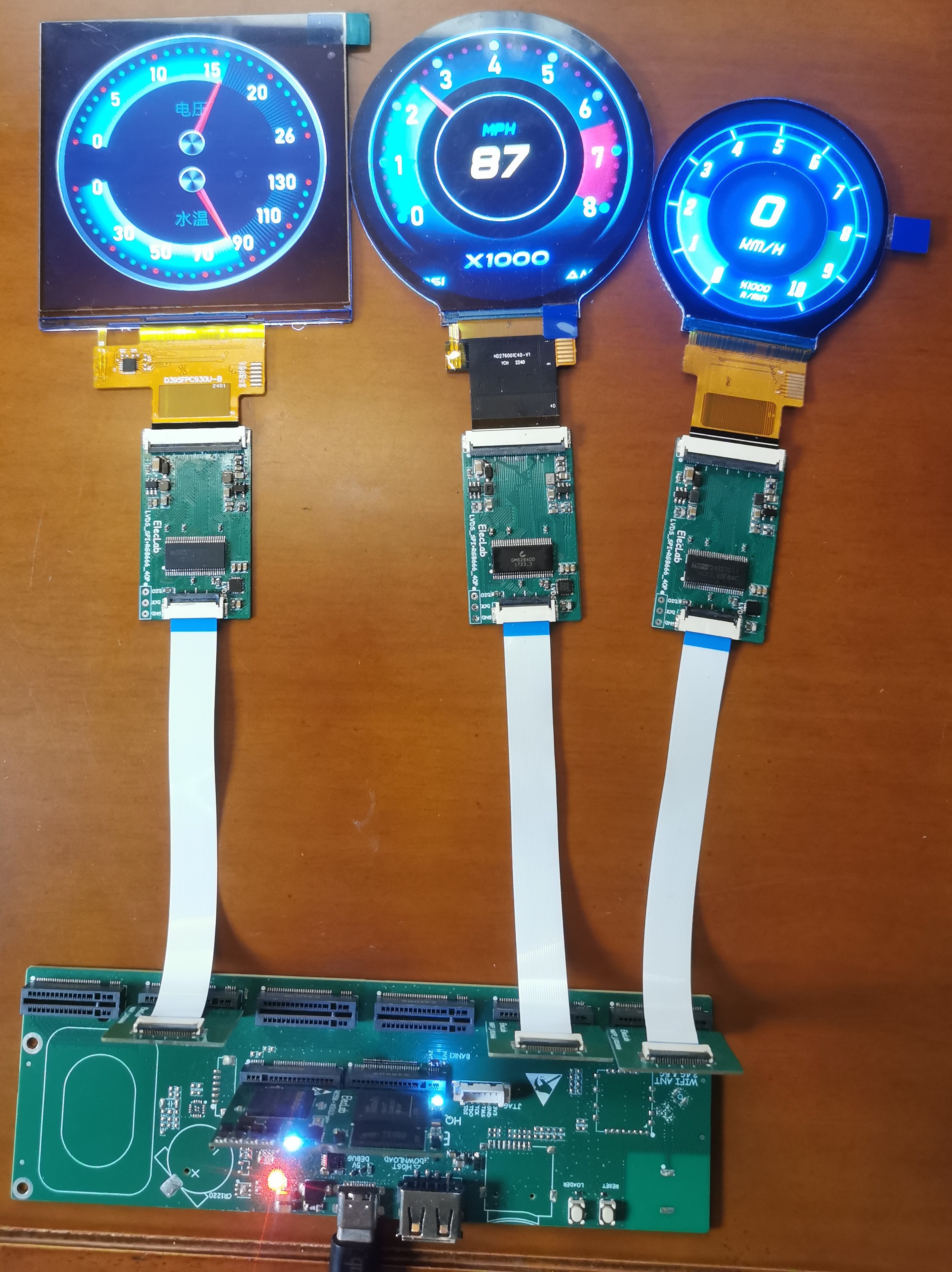
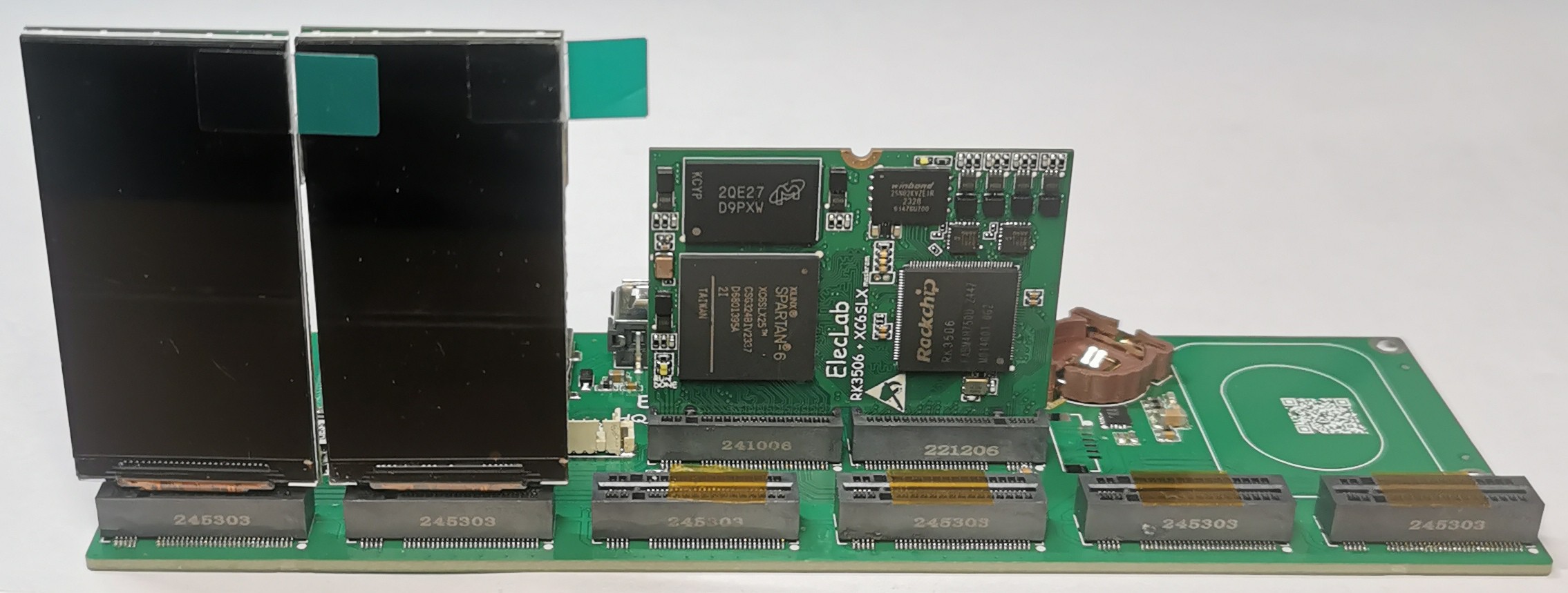
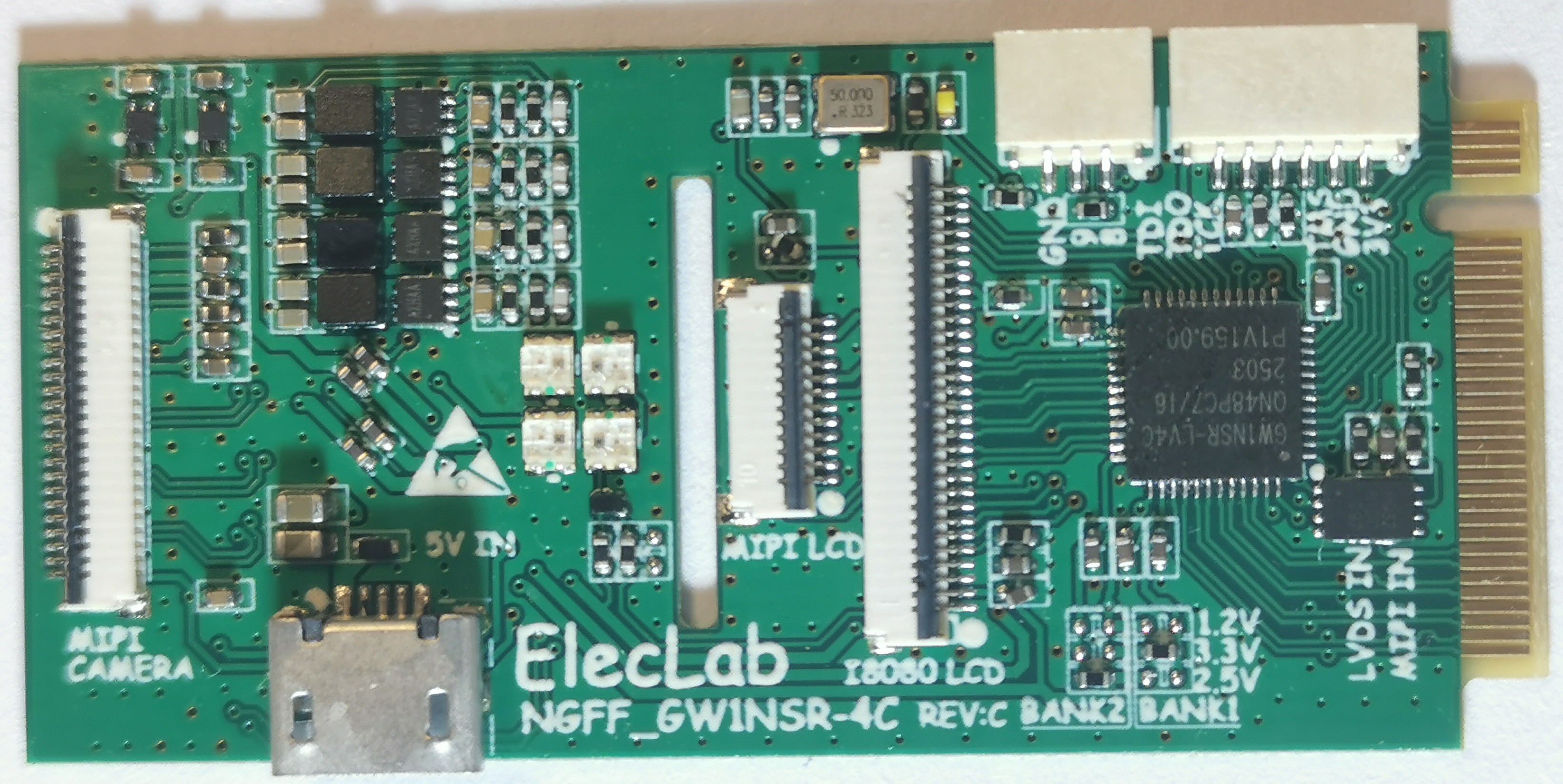
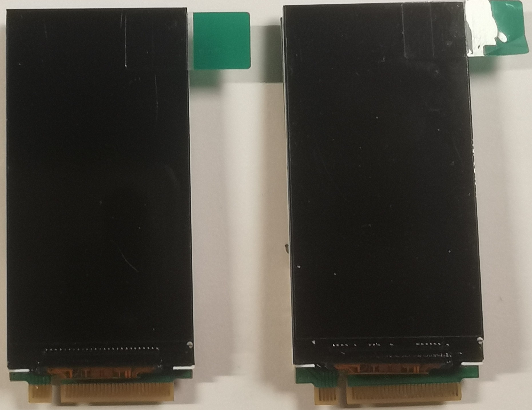
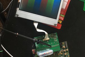
3. For the display part, we use GW1NSR-LV4CQN48 QFN48 package, which is a $2 and highly integrated FPGA chip. It has 4K LUT and 100MHz Cortex-M3 and 64Mb HyperRAM, MIP I IO can be output to the MIPI display and connect to the MIPI CSI camera. We used it to design a 1.9INCH 170x320 small display for Linux framebuffer. The whole display module uses a 6x1.9Inch display, which displays different areas under the same Framebuffer. Of course, we are also using it to design 1.54"/2.73" 320x320 MCU square display and 1.6" 400x400 MIPI circular display, and we are trying to integrate the OV5640 MIPI camera into this display module. All 6 displays receive Framebuffer cutting signals from ARM+FPGA boards through the LVDS interface.
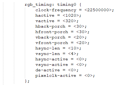
Set the framebuff with a resolution of 1020x320 on RK3506 and switch the reused IO pin from the DSMC function to RGB24.
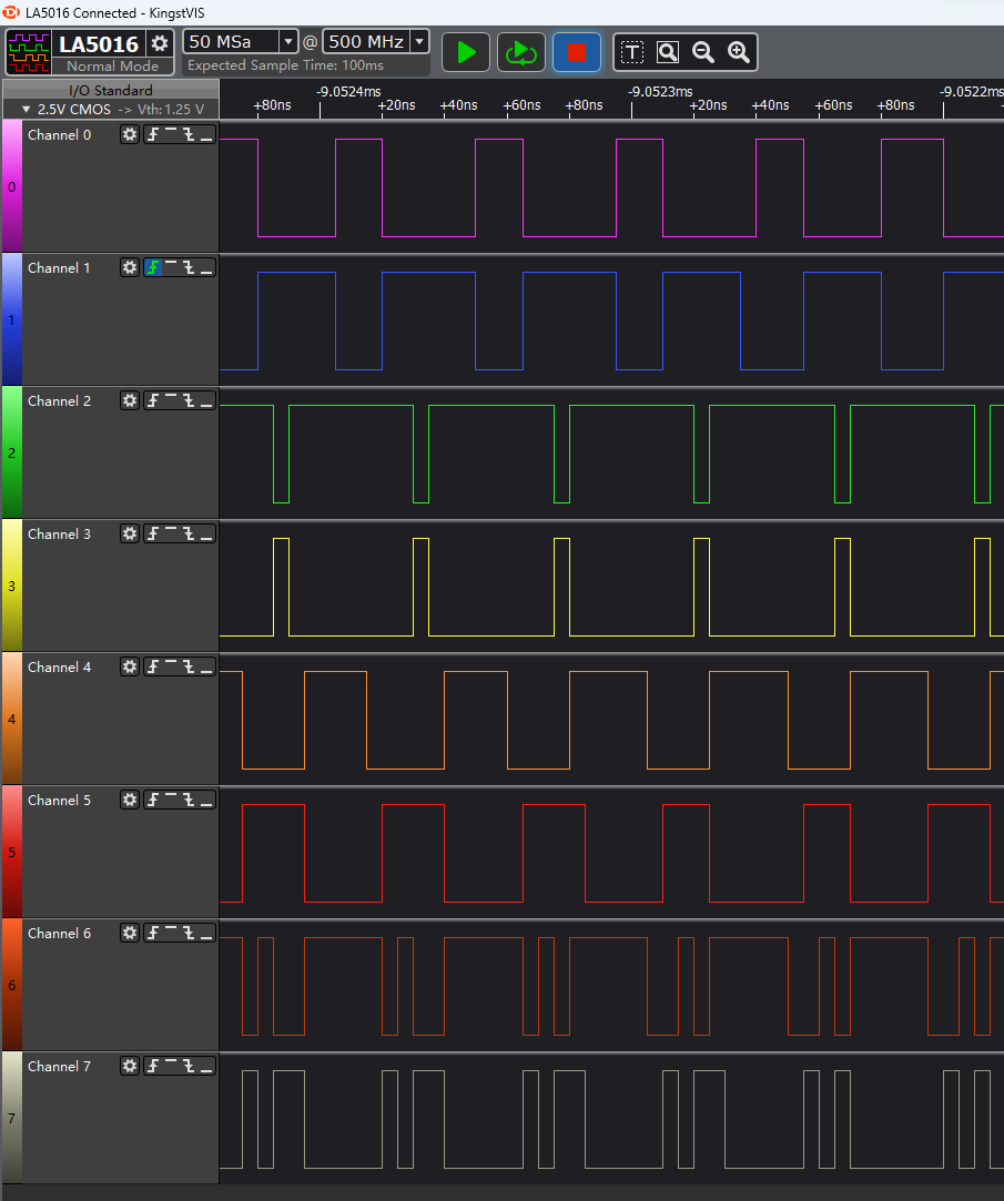
Create 6 rgb666->lvds data 3lanes modules on xc6slx25, verify its output, and test the PCB lvds signal with a logic analyzer..
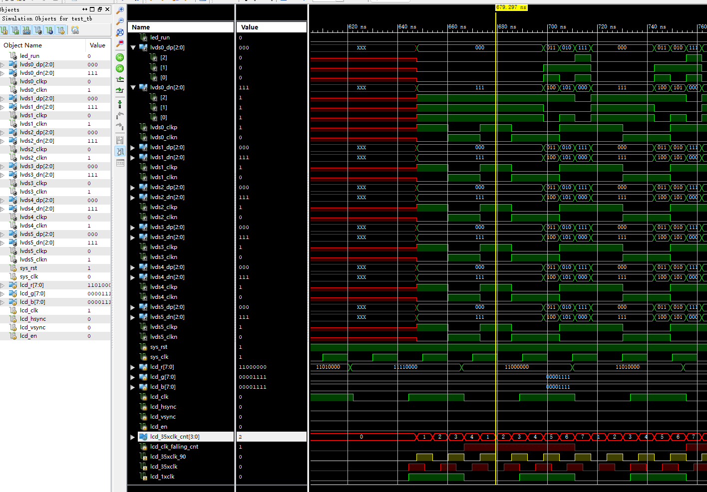
The lvds signals are decoded to RGB666 normally, and the next step is to display its contents on the MCU 8Bit 1.9" 170x320 LCD screen.
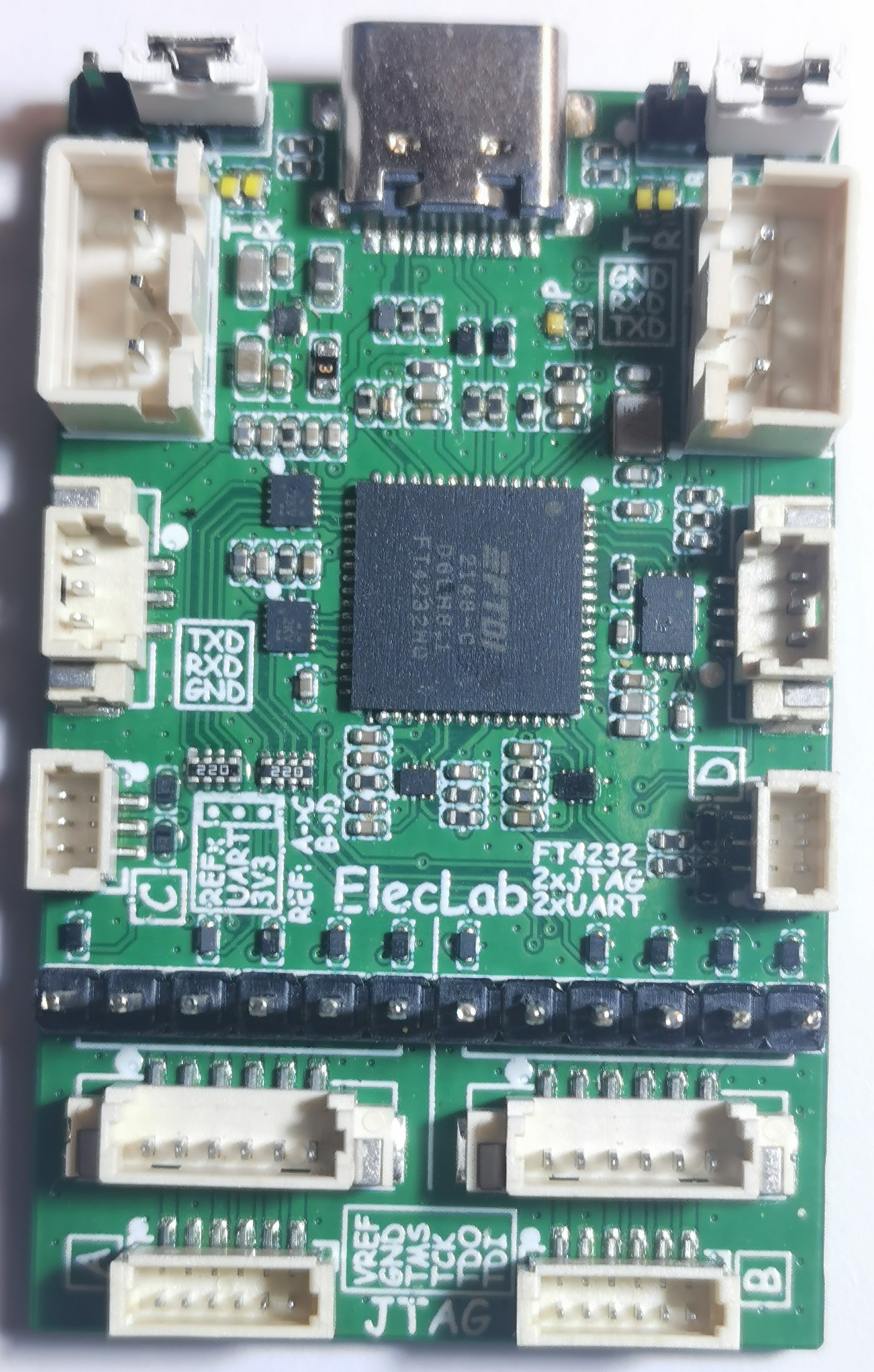
The FT4232HQ with two JTAG interfaces is very convenient. Maybe I can improve the FT4232HQ version of 4xJTAG. It will be great when multiple boards need to be tested!
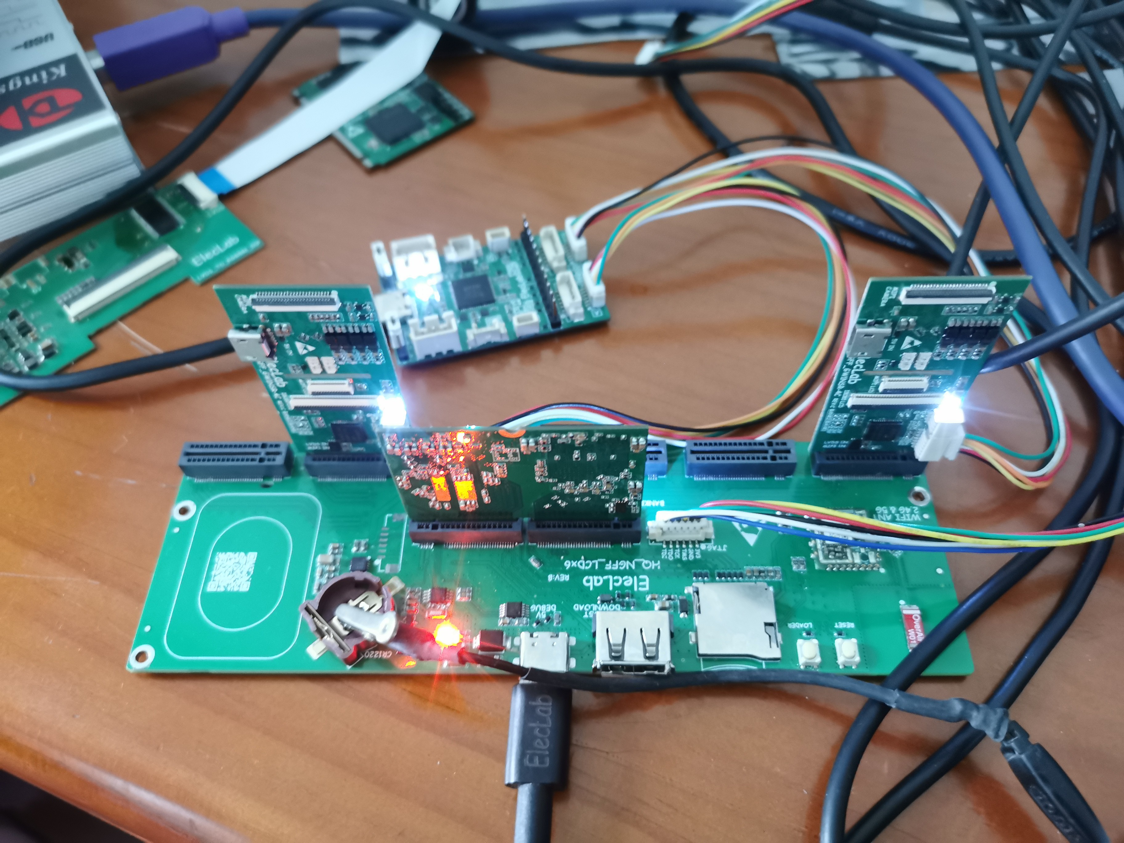
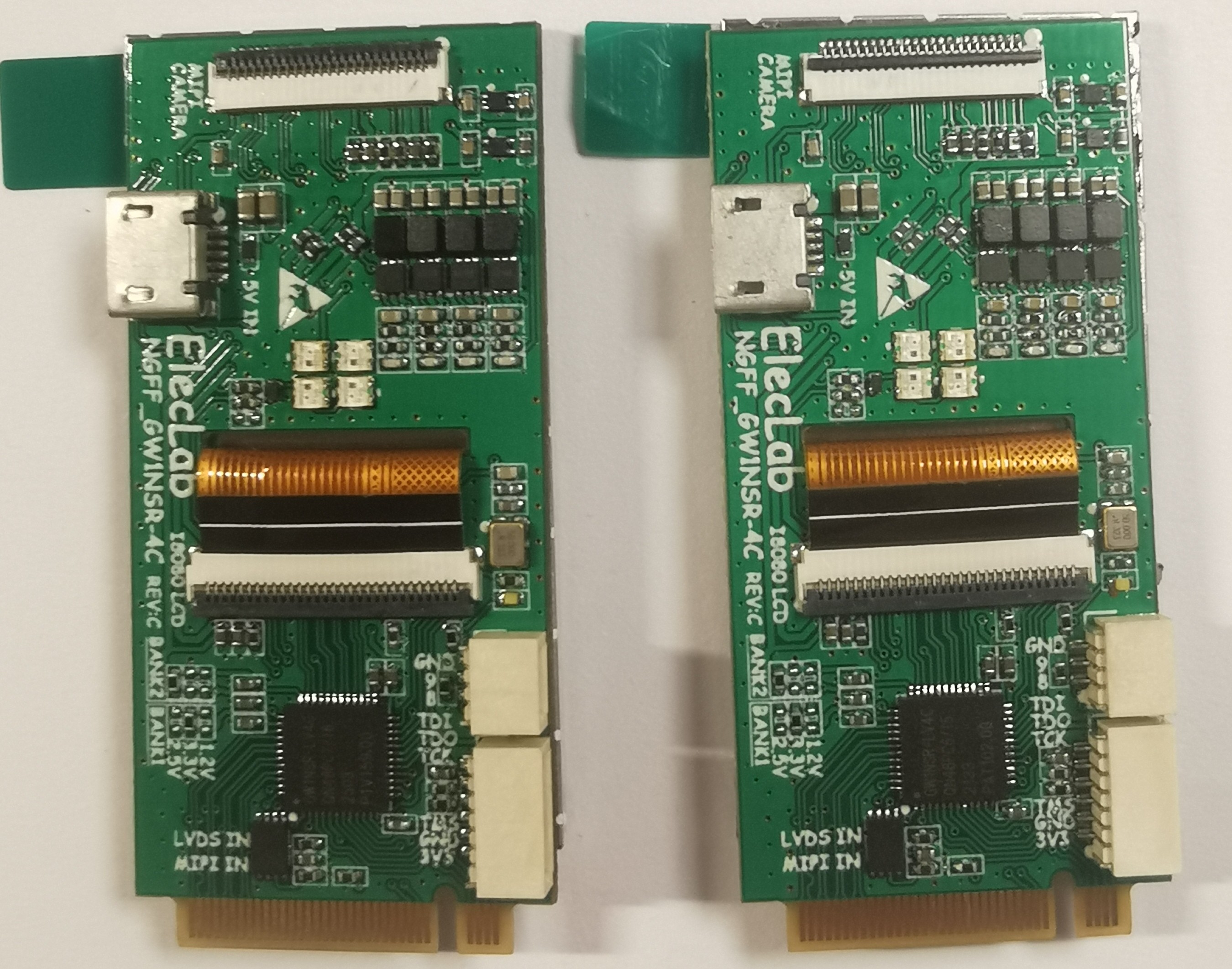
We have designed a new LCD screen adaptation board, which can be connected to a variety of small 40P LCD screens, including round screens, long strip screens and square screens.
3 lanes LVDS signal input, RGB666 signal output.
The FPGA board can drive six such displays, which is more suitable for some situations that require multiple small LCD screens, such as multi-meter displays.
The glow tube display program is designed using lvgl, which is set to a refresh rate of 20Hz due to the characteristics of the MCU screen.
Complete the 3 lanes lvds-> RGB666 PCB board, using a universal 40P RGB LCD interface, which can adapt to LCD screens of many sizes and resolutions.

 Wenting Zhang
 Dave
Dave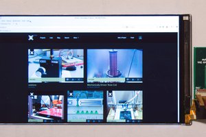
 twl
twl
 John Basista