 Stepan Skopivskiy
I have no experience writing interesting articles or stories, but the long story short is. I`m a Ukrainian who owns a US car after the incidents. I like Audi. My first car was a Q5 2015 MY. Logically (almost), the next choice happened to be an SQ5, preferably 20+ MY. After a few test drives, researching, and time, I was waiting for the new (used) car - Audi SQ5 Prestige 22MY.
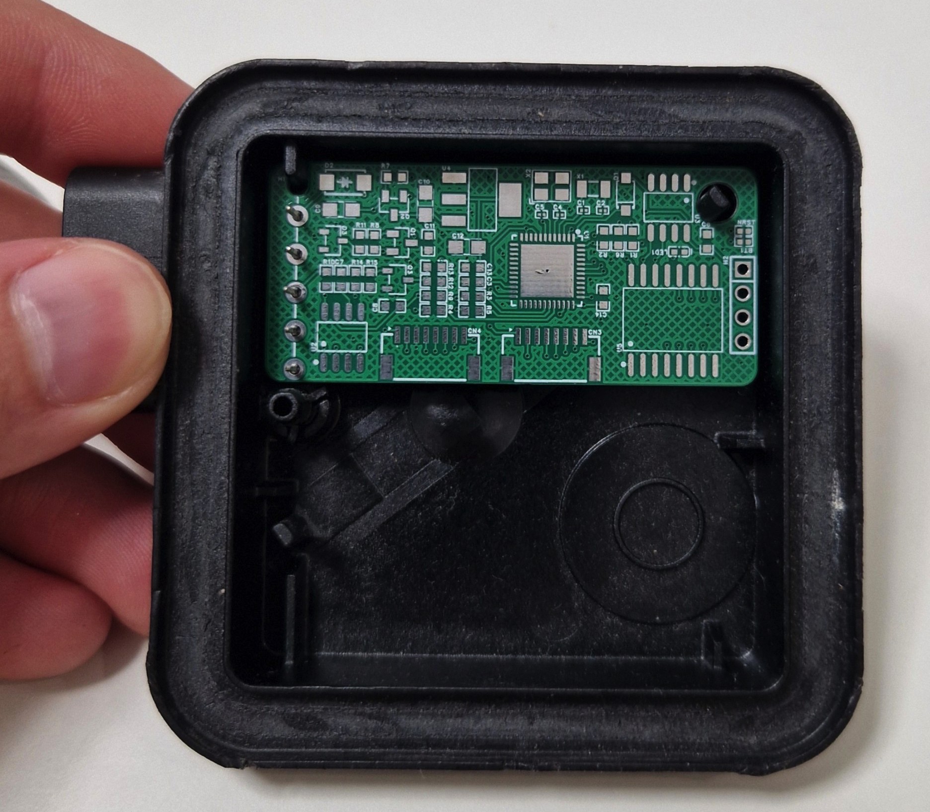
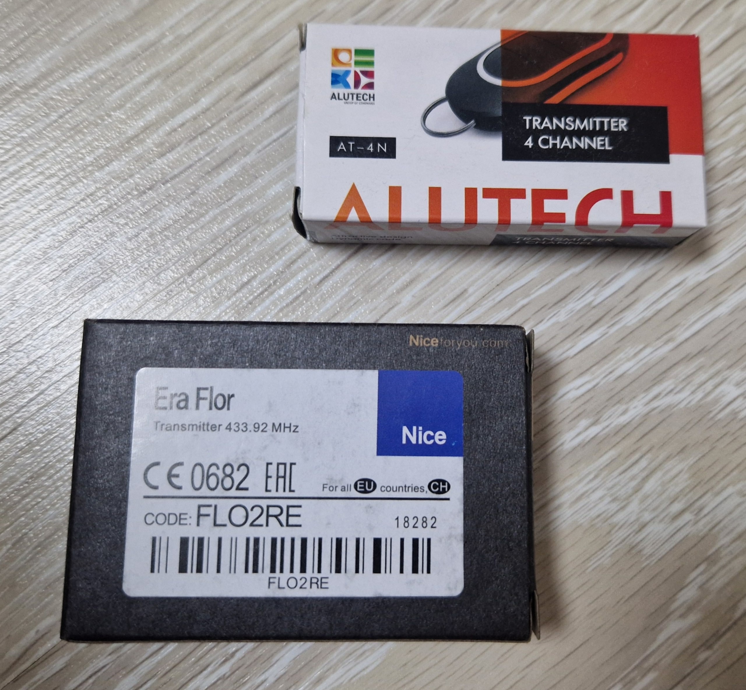
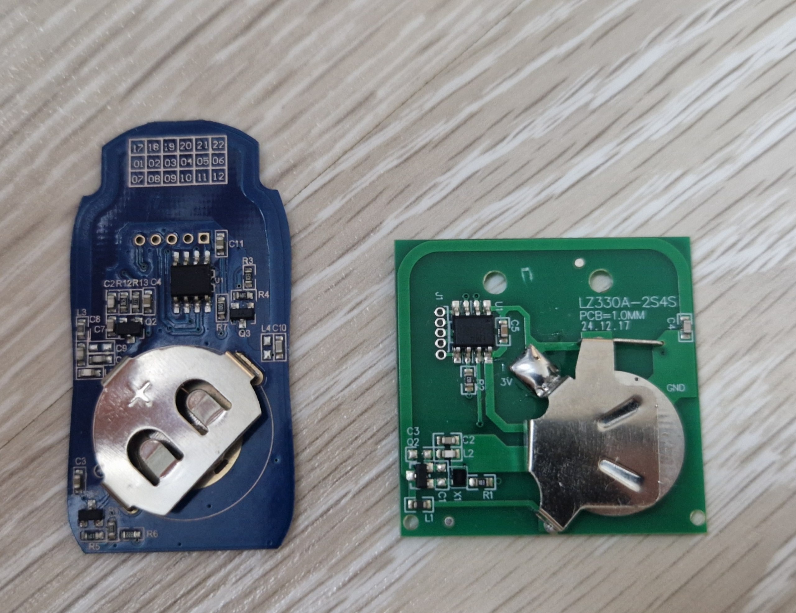
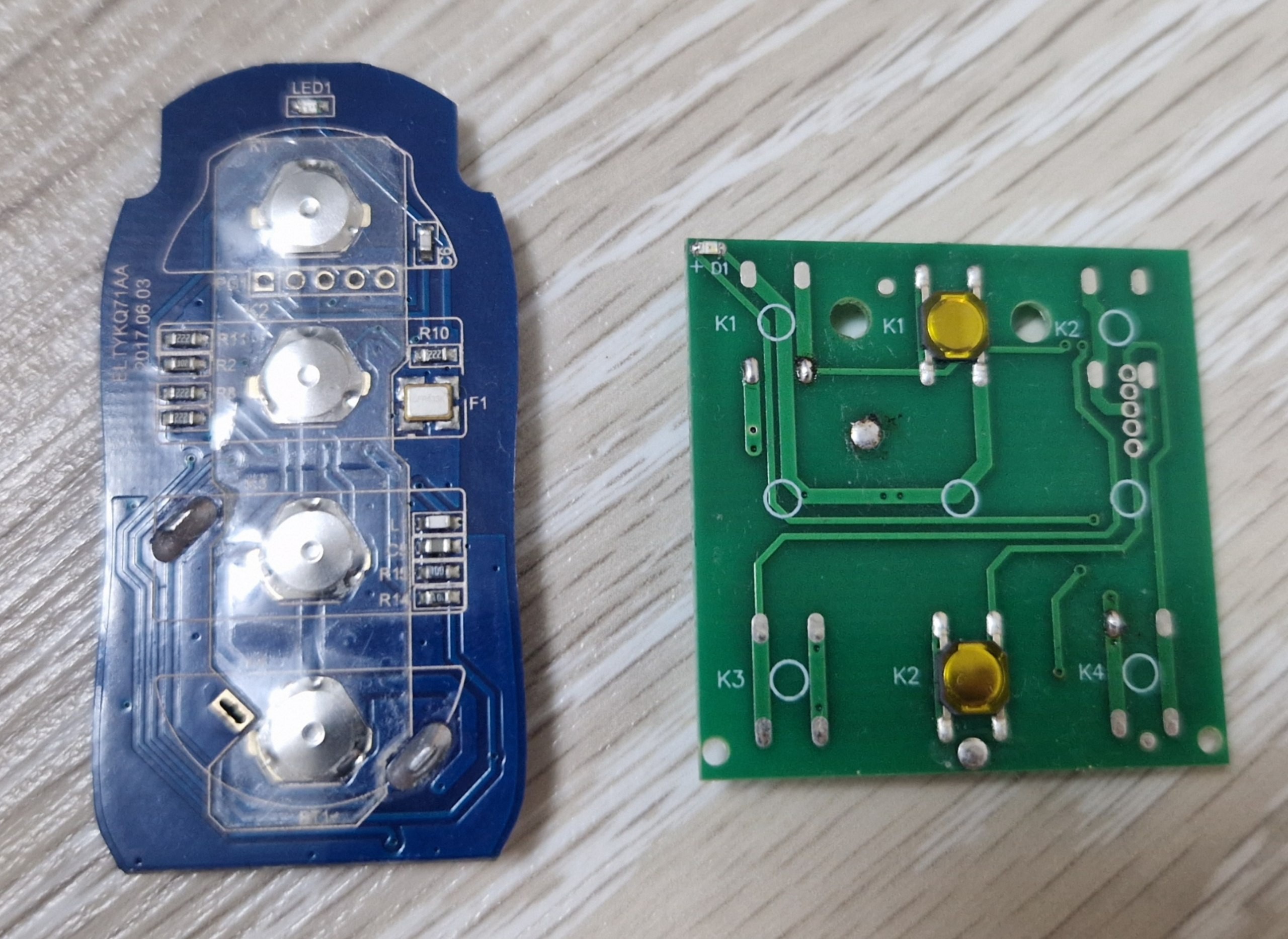
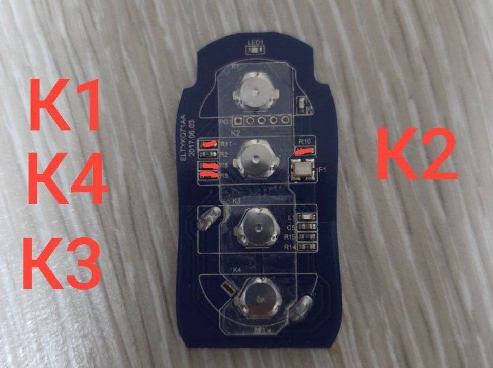
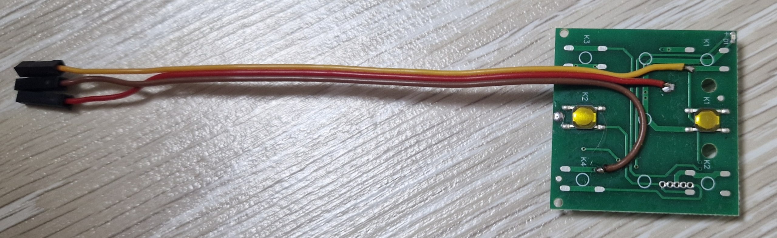
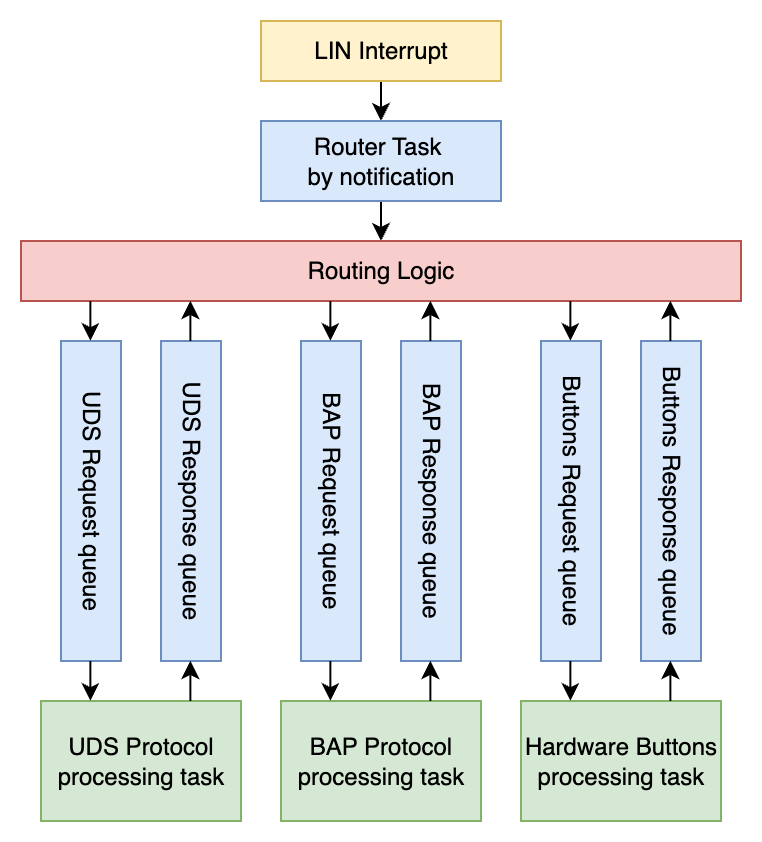
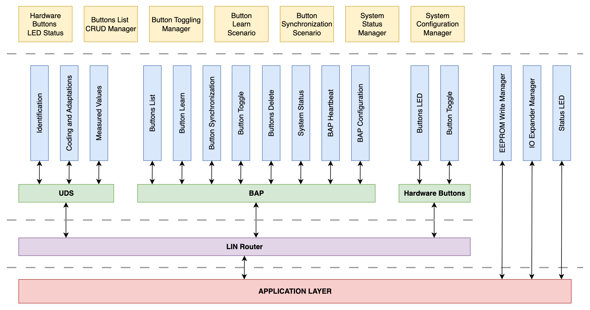
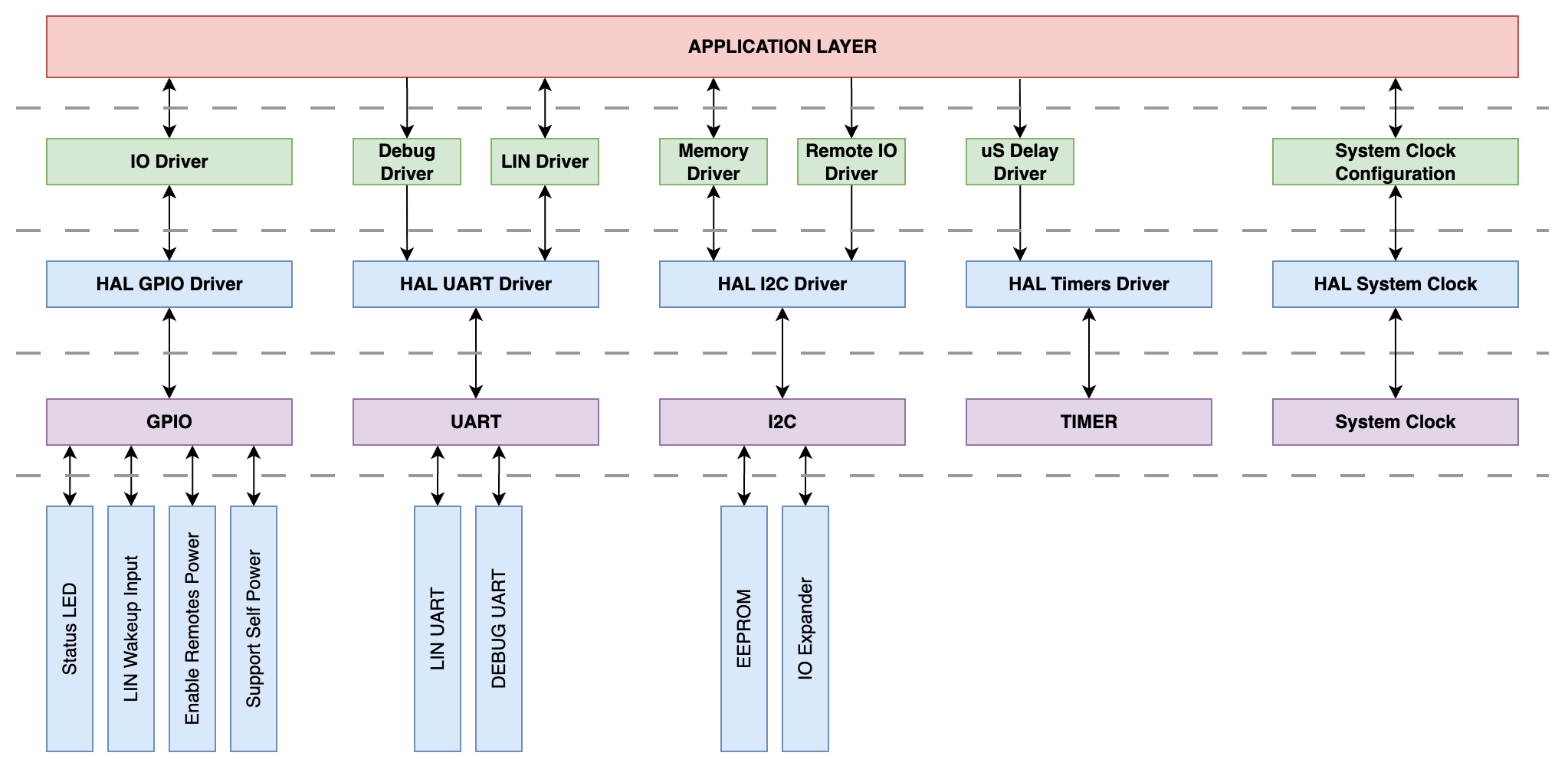
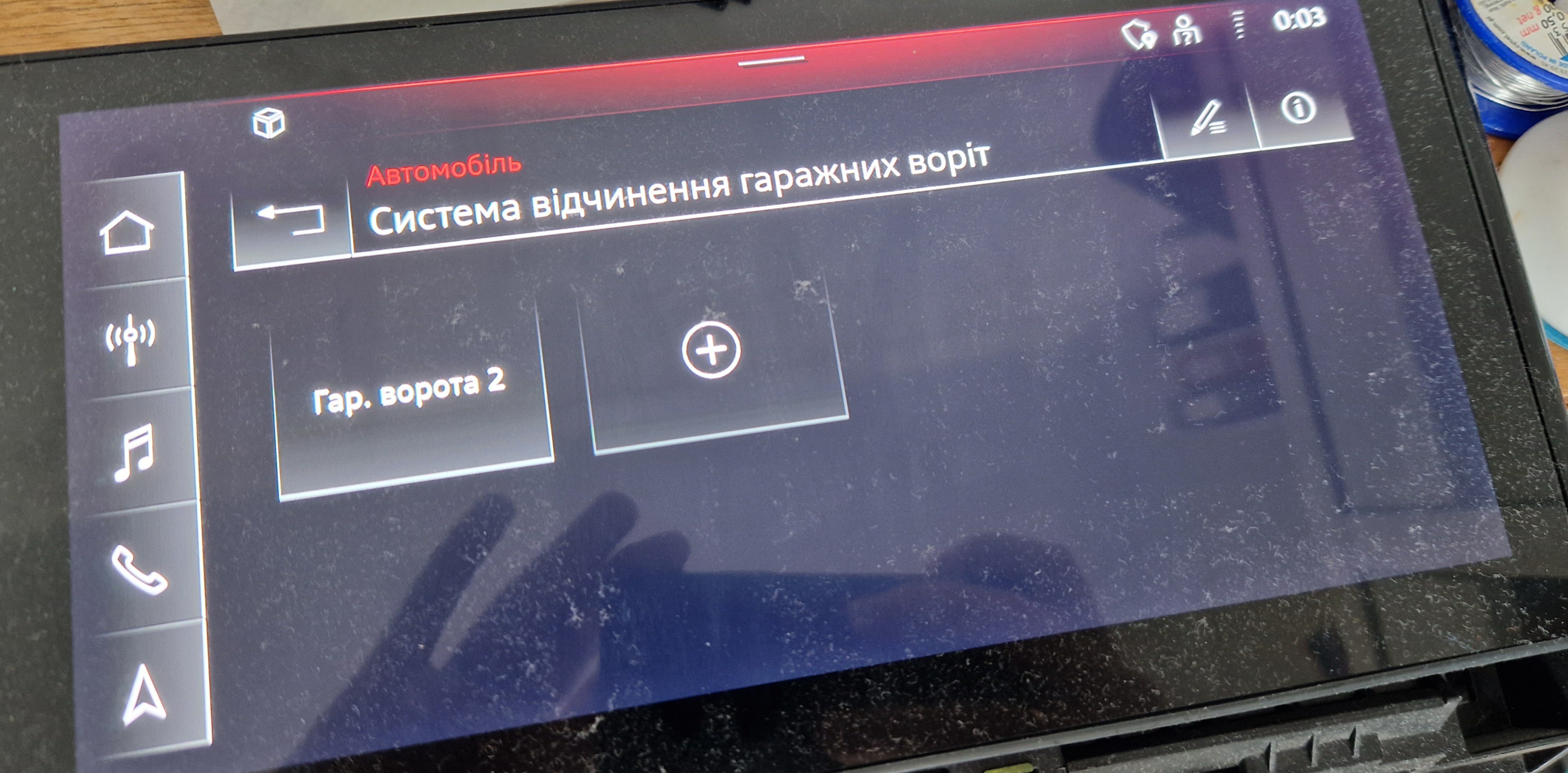
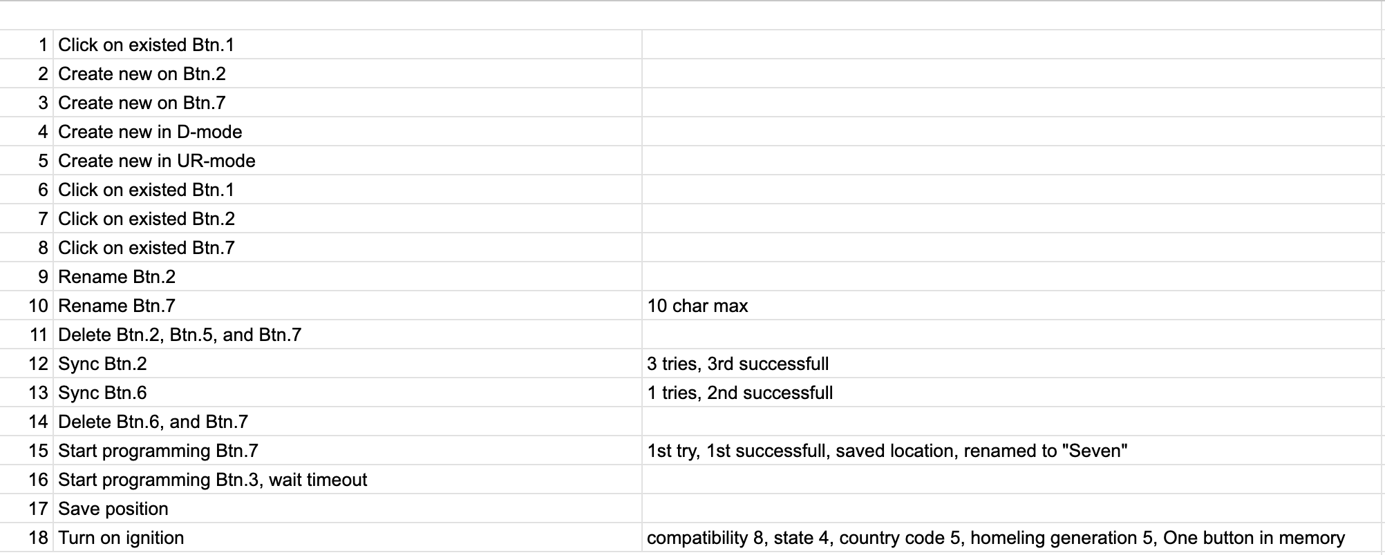
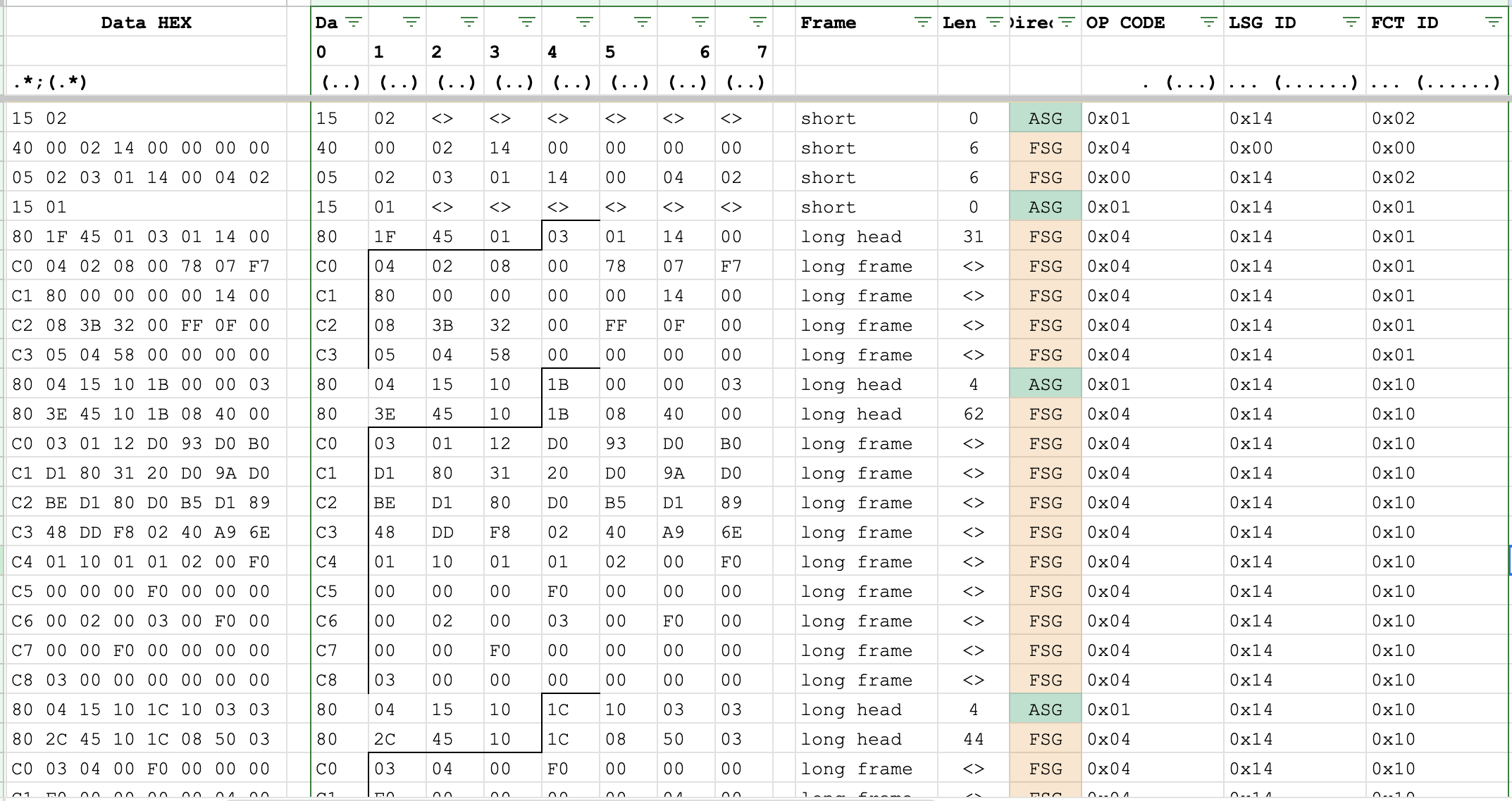
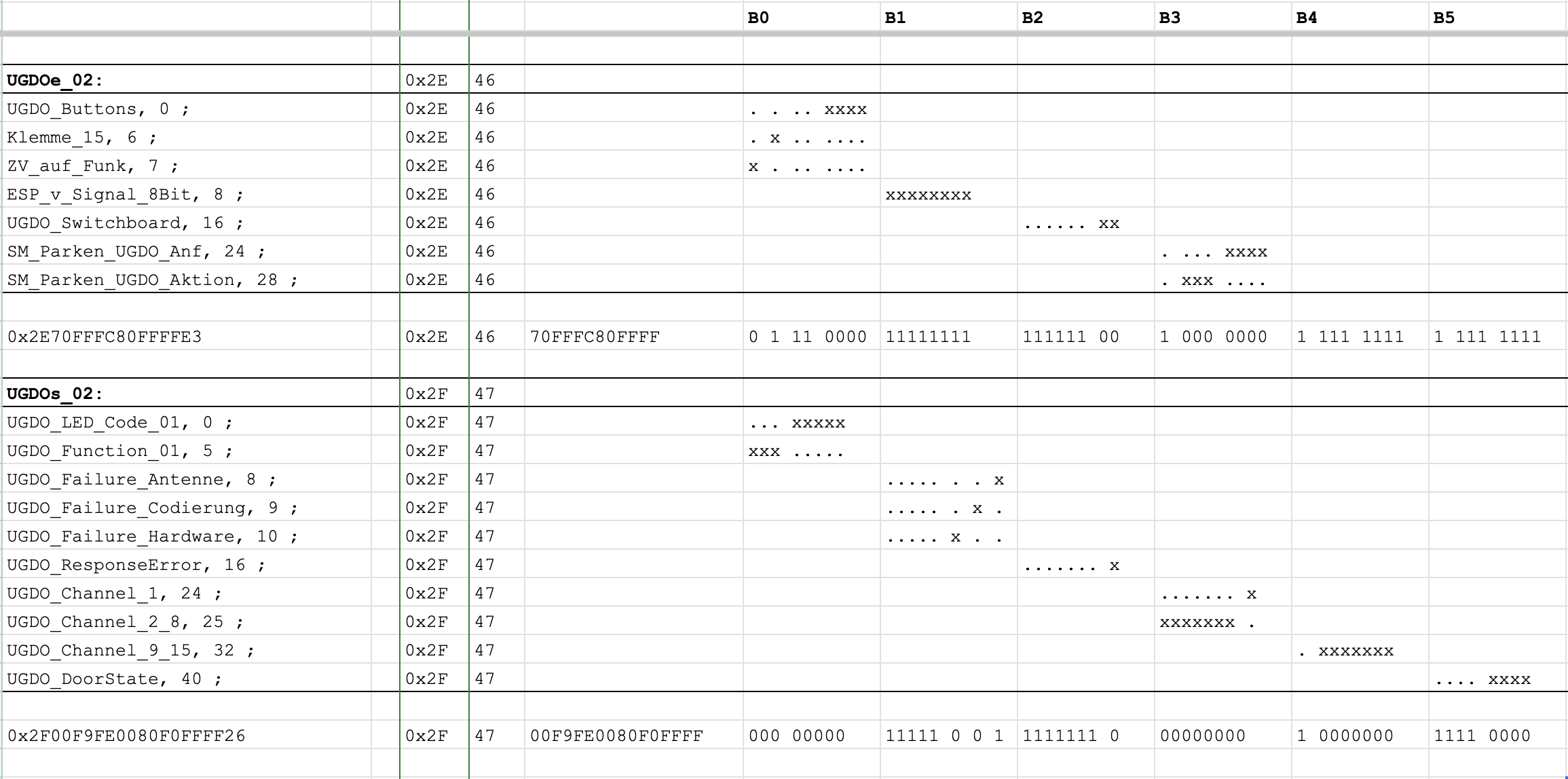
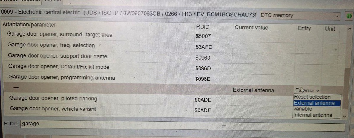
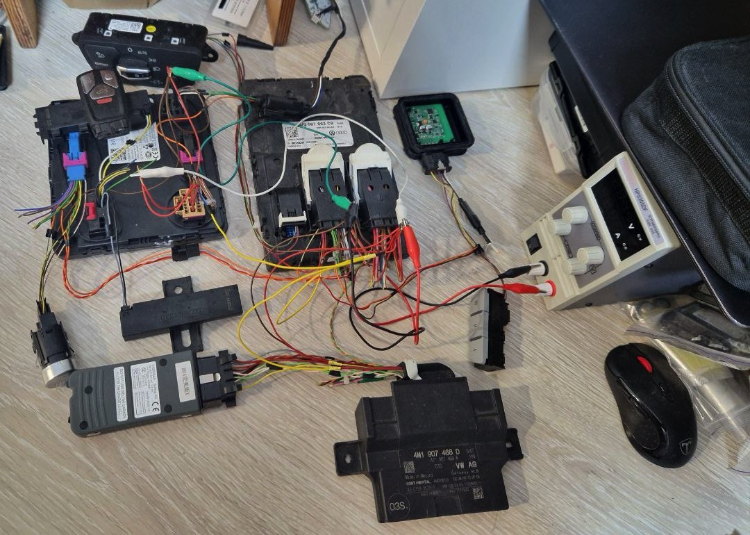
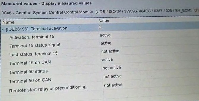
I live in a flat room without parking, but I own an underground one in the neighbourhood building. It has 2 levels of security access: barrier and garage door with one remote. Also, my new car had a Homelink option, the purpose of which was to simplify life. Unfortunately, the remote system of my parking was not compatible with HomeLink. The project starts here.

 Fluxly
 Enrico
 Valdez
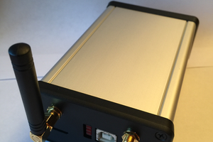
 David
David